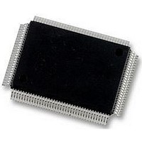
LM97593VH National Semiconductor, LM97593VH Datasheet - Page 3

LM97593VH
Manufacturer Part Number
LM97593VH
Description
12BIT ADC, 2CH, DDC/AGC, 128PQFP
Manufacturer
National Semiconductor
Datasheet
1.LM97593VH.pdf
(50 pages)
Specifications of LM97593VH
Resolution (bits)
12bit
Input Channel Type
Differential
Data Interface
Serial
Supply Voltage Range - Analogue
3V To 3.6V
Supply Voltage Range - Digital
1.6V To 2V, 3V To 3.6V
Supply
RoHS Compliant
Sampling Rate
65MSPS
Rohs Compliant
Yes
Lead Free Status / Rohs Status
Not Compliant
Available stocks
Company
Part Number
Manufacturer
Quantity
Price
Company:
Part Number:
LM97593VH/NOPB
Manufacturer:
VK
Quantity:
1 980
Company:
Part Number:
LM97593VH/NOPB
Manufacturer:
Texas Instruments
Quantity:
10 000
Pin No.
ANALOG I/O
13
27
14
26
21
15
24
16
23
17
22
8
DIGITAL I/O
30
45
82
78
127:125
40:42
124
43
80
Pin Descriptions and Equivalent Circuits
Symbol
V
V
V
V
V
V
V
V
V
V
V
REFSEL/DCS
PD
MR
AOUT
BOUT
AGAIN[2:0]
BGAIN[2:0]
ASTROBE
BSTROBE
SCK
IN
IN
IN
IN
REF
COM
COM
RP
RP
RN
RN
A−
B−
A+
B+
A
B
A
B
A
B
Equivalent Circuit
Analog Input
Analog Input
Control / Analog Input
Analog Output
Analog Output
Analog Output
Control Input
Input
Input
Output
Output
Output
Output
Description
Negative differential input signal for the 'A' channel
Negative differential input signal for the 'B' channel
Positive differential input signal for the 'A' channel
Positive differential input signal for the 'B' channel
Reference Select Pin / External Reference Voltage Input
Input differential full scale swing = 2 * V
Common Mode reference voltage for the 'A' channel
Common Mode reference voltage for the 'B' channel
These pins may be loaded to 1 mA for use as temperature stable 1.5V
references.
Upper reference voltage for the 'A' channel
Upper reference voltage for the 'B' channel
Lower reference voltage for the 'A' channel
Lower reference voltage for the 'B' channel
This is a three-state pin. V
REFSEL/DCS = AGND: the internal reference is enabled and duty cycle
REFSEL/DCS = V
REFSEL/DCS = V
POWER DOWN, when high both ADCs are powered down, when low,
both ADCs are enabled
MASTER RESET, Active low
Resets all registers within the chip. ASTROBE and BSTROBE are
asserted during MR.
SERIAL OUTPUT DATA, Active high
The 2's complement serial output data is transmitted on these pins, MSB
first. The output bits change on the rising edge of SCK (falling edge if
SCK_POL=1) and should be captured on the falling edge of SCK (rising
if SCK_POL=1). These pins are tri-stated at power up and are enabled
by the SOUT_EN control register bit. See Figure 13 and Figure 34 timing
diagrams. In Debug Mode AOUT=DEBUG[1], BOUT=DEBUG[0].
OUTPUT DATA TO DVGA, Active high
3 bit bus that sets the gain of the DVGA determined by the AGC circuit.
DVGA STROBE, Active low
Strobes the data into the DVGA. See Figure 7 and Figure 41 timing
diagrams.
SERIAL DATA CLOCK, Active high or low
The serial data is clocked out of the chip by this clock. The active edge
of the clock is user programmable. This pin is tri-stated at power up and
is enabled by the SOUT_EN control register bit. See Figure 13 and
Figure 34 timing diagrams. In Debug Mode outputs an appropiate clock
for the debug data. If RATE=0 the input CK duty cycle will be reflected
to SCK.
V
V
correction is applied to the ADC input clock (CK).
cycle correction is applied to the ADC input clock (CK).
A 0.8-1.2V external reference to the V
3
REF
REF
= V
= 0.8V to 1.5V:
A
to V
A
A
COM
- 0.3V:
: DCS is on, the internal reference is disabled. Apply
: the internal reference is enabled and no duty
COM
Reference Voltage = 1.0 V (Internal)
Reference Voltage = V
= V
COM
A or V
REF
REF
pin.
COM
B.
REF
(External)
www.national.com


