LIS302DLH STMicroelectronics, LIS302DLH Datasheet - Page 28
LIS302DLH
Manufacturer Part Number
LIS302DLH
Description
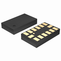
SENSOR ACCELEROMETER 3AXIS 14LGA
Manufacturer
STMicroelectronics
Datasheet
1.LIS302DLH.pdf
(37 pages)
Specifications of LIS302DLH
Featured Product
STM32 Cortex-M3 Companion Products
Axis
X, Y, Z
Acceleration Range
±2.3g, 9.2g
Sensitivity
18mg/digit, 72mg/digit
Voltage - Supply
2.16 V ~ 3.6 V
Output Type
Digital
Bandwidth
100Hz ~ 400Hz Selectable
Interface
I²C, SPI
Mounting Type
Surface Mount
Package / Case
14-LGA
Package Type
LGA
Operating Supply Voltage (min)
2.16V
Operating Supply Voltage (typ)
2.5V
Operating Supply Voltage (max)
3.6V
Operating Temperature (min)
-40C
Operating Temperature (max)
85C
Operating Temperature Classification
Industrial
Product Depth (mm)
3mm
Product Height (mm)
0.92mm
Product Length (mm)
5mm
Mounting
Surface Mount
Pin Count
14
Sensing Axis
Triple
Acceleration
2 g, 4 g, 8 g
Digital Output - Number Of Bits
16 bit
Supply Voltage (max)
3.6 V
Supply Voltage (min)
2.16 V
Maximum Operating Temperature
+ 85 C
Minimum Operating Temperature
- 40 C
Digital Output - Bus Interface
I2C, SPI
Lead Free Status / RoHS Status
Lead free / RoHS Compliant
Other names
497-10052
Available stocks
Company
Part Number
Manufacturer
Quantity
Price
Company:

Part Number:
LIS302DLHS0.5
Manufacturer:
INNOLUX
Quantity:
1 000
Company:
Part Number:
LIS302DLHTR
Manufacturer:
SANYO
Quantity:
11


Register description
7.6
28/37
Table 29.
BDU bit is used to inhibit output registers update between the reading of upper and lower
register parts. In default mode (BDU = ‘0’) the lower and upper register parts are updated
continuously. If it is not sure to read faster than output data rate, it is recommended to set
BDU bit to ‘1’. In this way, after the reading of the lower (upper) register part, the content of
that output registers is not updated until the upper (lower) part is read too.
This feature avoids reading LSB and MSB related to different samples.
CTRL_REG5 (24h)
Table 30.
Table 31.
TurnOn bits are used for turning on the sleep to wake function.
Table 32.
Setting TurnOn[1:0] bits to 11 the “sleep to wake” function is enabled. When an interrupt
event occurs the device is turned to normal mode increasing the ODR to the value defined in
BDU
BLE
FS1, FS0
STsign
ST
SIM
TurnOn1,
TurnOn0
TurnOn1
0
0
1
CTRL_REG4 description
CTRL_REG5 register
CTRL_REG5 description
Sleep to wake configuration
Block data update. Default value: 0
(0: continuos update; 1: output registers not updated between MSB and LSB reading)
Big/little endian data selection. Default value 0.
(0: data LSB @ lower address; 1: data MSB @ lower address)
Full-scale selection. Default value: 00.
(00: ±2 g; 01: ±4 g; 11: ±8 g)
Self-test sign. Default value: 00.
(0: self-test plus; 1 self-test minus)
Self-test enable. Default value: 0.
(0: self-test disabled; 1: self-test enabled)
SPI serial interface mode selection. Default value: 0.
(0: 4-wire interface; 1: 3-wire interface)
Turn-on mode selection for sleep to wake function. Default value: 00.
0
TurnOn0
0
1
0
Doc ID 15797 Rev 1
Turned on: The device is in low power mode (ODR is defined in
0
Sleep to wake function is disabled
Sleep to wake status
0
CTRL_REG1)
0
TurnOn1
LIS302DLH
TurnOn0
Related parts for LIS302DLH
Image
Part Number
Description
Manufacturer
Datasheet
Request
R

Part Number:
Description:
STMicroelectronics [RIPPLE-CARRY BINARY COUNTER/DIVIDERS]
Manufacturer:
STMicroelectronics
Datasheet:
Part Number:
Description:
STMicroelectronics [LIQUID-CRYSTAL DISPLAY DRIVERS]
Manufacturer:
STMicroelectronics
Datasheet:

Part Number:
Description:
BOARD EVAL FOR MEMS SENSORS
Manufacturer:
STMicroelectronics
Datasheet:
Part Number:
Description:
NPN TRANSISTOR POWER MODULE
Manufacturer:
STMicroelectronics
Datasheet:
Part Number:
Description:
TURBOSWITCH ULTRA-FAST HIGH VOLTAGE DIODE
Manufacturer:
STMicroelectronics
Datasheet:
Part Number:
Description:
Manufacturer:
STMicroelectronics
Datasheet:
Part Number:
Description:
DIODE / SCR MODULE
Manufacturer:
STMicroelectronics
Datasheet:
Part Number:
Description:
DIODE / SCR MODULE
Manufacturer:
STMicroelectronics
Datasheet:
Part Number:
Description:
Search -----> STE16N100
Manufacturer:
STMicroelectronics
Datasheet:
Part Number:
Description:
Search ---> STE53NA50
Manufacturer:
STMicroelectronics
Datasheet:
Part Number:
Description:
NPN Transistor Power Module
Manufacturer:
STMicroelectronics
Datasheet:
Part Number:
Description:
DIODE / SCR MODULE
Manufacturer:
STMicroelectronics
Datasheet: