LIS35DETR STMicroelectronics, LIS35DETR Datasheet - Page 19
LIS35DETR
Manufacturer Part Number
LIS35DETR
Description
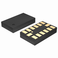
IC ACCELEROMETER 3AXIS 14LGA
Manufacturer
STMicroelectronics
Datasheet
1.LIS35DETR.pdf
(39 pages)
Specifications of LIS35DETR
Axis
X, Y, Z
Acceleration Range
±2.3g, 9.2g
Sensitivity
18mg/digit, 72mg/digit
Voltage - Supply
2.16 V ~ 3.6 V
Output Type
Digital
Bandwidth
100Hz ~ 400Hz Selectable
Interface
I²C, SPI
Mounting Type
Surface Mount
Package / Case
14-LGA
Sensing Axis
X, Y, Z
Acceleration
2 g, 8 g
Digital Output - Number Of Bits
8 bit
Supply Voltage (max)
3.6 V
Supply Voltage (min)
2.16 V
Supply Current
0.3 mA
Maximum Operating Temperature
+ 85 C
Minimum Operating Temperature
- 40 C
Digital Output - Bus Interface
I2C, SPI
Mounting Style
SMD/SMT
Shutdown
Yes
Lead Free Status / RoHS Status
Lead free / RoHS Compliant
Available stocks
Company
Part Number
Manufacturer
Quantity
Price

Part Number:
LIS35DETR
Manufacturer:
ST
Quantity:
20 000


LIS35DE
5.2
Table 12.
Table 13.
Table 14.
Table 15.
Data are transmitted in byte format (DATA). Each data transfer contains 8 bits. The number
of bytes transferred per transfer is unlimited. Data is transferred with the Most Significant bit
(MSb) first. If a receiver can’t receive another complete byte of data until it has performed
some other function, it can hold the clock line, SCL LOW to force the transmitter into a wait
state. Data transfer only continues when the receiver is ready for another byte and releases
the data line. If a slave receiver doesn’t acknowledge the slave address (i.e. it is not able to
receive because it is performing some real time function) the data line must be left HIGH by
the slave. The Master can then abort the transfer. A LOW to HIGH transition on the SDA line
while the SCL line is HIGH is defined as a STOP condition. Each data transfer must be
terminated by the generation of a STOP (SP) condition.
In order to read multiple bytes, it is necessary to assert the most significant bit of the sub-
address field. In other words, SUB(7) must be equal to 1 while SUB(6-0) represents the
address of first register to read.
In the presented communication format MAK is Master Acknowledge and NMAK is No
Master Acknowledge.
SPI bus interface
The LIS35DE SPI is a bus slave. The SPI allows to write and read the registers of the
device.
The Serial Interface interacts with the outside world with 4 wires: CS, SPC, SDI and SDO.
Master
Master
Master
Slave
Slave
Slave
Master
Slave
ST
ST
ST
Transfer when Master is writing multiple bytes to slave
Transfer when Master is receiving (reading) one byte of data from slave
Transfer when Master is receiving (reading) multiple bytes of data from
slave
Transfer when Master is receiving (reading) multiple bytes of data from
slave
SAD + W
SAD + W
SAD + W
DATA
SAK
SAK
SAK
Doc ID 15594 Rev 1
SUB
SUB
SUB
MAK
SAK
SAK
SAK
SR
SR
SAD + R
DATA
DATA
SAD + R
SAK
SAK
SAK
NMAK
DATA
DATA
Digital interfaces
DATA
NMAK
SAK
SP
MAK
19/39
SP
SP
Related parts for LIS35DETR
Image
Part Number
Description
Manufacturer
Datasheet
Request
R

Part Number:
Description:
STMicroelectronics [RIPPLE-CARRY BINARY COUNTER/DIVIDERS]
Manufacturer:
STMicroelectronics
Datasheet:
Part Number:
Description:
STMicroelectronics [LIQUID-CRYSTAL DISPLAY DRIVERS]
Manufacturer:
STMicroelectronics
Datasheet:

Part Number:
Description:
BOARD EVAL FOR MEMS SENSORS
Manufacturer:
STMicroelectronics
Datasheet:
Part Number:
Description:
NPN TRANSISTOR POWER MODULE
Manufacturer:
STMicroelectronics
Datasheet:
Part Number:
Description:
TURBOSWITCH ULTRA-FAST HIGH VOLTAGE DIODE
Manufacturer:
STMicroelectronics
Datasheet:
Part Number:
Description:
Manufacturer:
STMicroelectronics
Datasheet:
Part Number:
Description:
DIODE / SCR MODULE
Manufacturer:
STMicroelectronics
Datasheet:
Part Number:
Description:
DIODE / SCR MODULE
Manufacturer:
STMicroelectronics
Datasheet:
Part Number:
Description:
Search -----> STE16N100
Manufacturer:
STMicroelectronics
Datasheet:
Part Number:
Description:
Search ---> STE53NA50
Manufacturer:
STMicroelectronics
Datasheet:
Part Number:
Description:
NPN Transistor Power Module
Manufacturer:
STMicroelectronics
Datasheet:
Part Number:
Description:
DIODE / SCR MODULE
Manufacturer:
STMicroelectronics
Datasheet: