ADIS16204BCCZ Analog Devices Inc, ADIS16204BCCZ Datasheet - Page 18
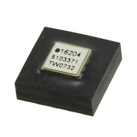
ADIS16204BCCZ
Manufacturer Part Number
ADIS16204BCCZ
Description
IC ACCEL DIGITAL HI-G 16-LGA
Manufacturer
Analog Devices Inc
Datasheet
1.ADIS16204PCBZ.pdf
(24 pages)
Specifications of ADIS16204BCCZ
Acceleration Range
±37g, 70g
Axis
X, Y
Sensitivity
17.125 LSB/mg, 8.407 LSB/mg
Voltage - Supply
3 V ~ 3.6 V
Output Type
Digital
Bandwidth
400Hz
Interface
SPI
Mounting Type
Surface Mount
Package / Case
16-LGA
No. Of Axes
2
Sensor Case Style
LGA
No. Of Pins
16
Supply Voltage Range
3V To 3.6V
Operating Temperature Range
-40°C To +105°C
Svhc
No SVHC (18-Jun-2010)
Family Name
ADIS16204
Package Type
LGA
Operating Supply Voltage (min)
3V
Operating Supply Voltage (typ)
3.3V
Operating Supply Voltage (max)
3.6V
Operating Temperature (min)
-40C
Operating Temperature (max)
105C
Operating Temperature Classification
Industrial
Product Depth (mm)
8mm
Product Height (mm)
5.2mm
Product Length (mm)
8mm
Mounting
Surface Mount
Pin Count
16
Interface Type
SPI
Sensitivity Per Axis
17.125mg / LSB
Rohs Compliant
Yes
Lead Free Status / RoHS Status
Lead free / RoHS Compliant
For Use With
ADIS16204/PCBZ - BOARD EVAL FOR ADIS16204/PCB
Lead Free Status / Rohs Status
Compliant
Available stocks
Company
Part Number
Manufacturer
Quantity
Price
Company:

Part Number:
ADIS16204BCCZ
Manufacturer:
ST
Quantity:
390


ADIS16204
STATUS Conditions
The STATUS register contains the following error-condition
flags: alarm conditions, self-test status, SPI communication
failure, capture buffer full, control register update failure, and
power supply out of range. See Table 27 and Table 28 for the
appropriate register access and bit assignment for each flag.
The bits assigned for checking power supply range automati-
cally reset to zero when the error condition no longer exists.
Clearing the remaining error-flag bits requires a single write
command to the COMMAND register (write a 1 to Bit 4).
See Table 8 and Table 9 for the configuration details of the
COMMAND register. If the error condition still exists after
exercising the COMMAND register to clear the bits, the appro-
priate error flag bit returns to 1 during the next sampling cycle.
All bits in the STATUS register are volatile.
Table 27. STATUS Register Definition
Address
0x3D, 0x3C
Table 28. STATUS Bit Descriptions
Bit
15:13
12
11:10
9
8
7:6
5
4
3
2
1
0
ALARM DETECTION AND EVENT CAPTURE
The ADIS16204 provides alarm detection and event capture
functions, which monitor critical internal and external
operating conditions. Six factory standard alarms monitor
the AIDS16204 for normal operation. Two programmable
alarms provide monitoring for system-critical conditions,
Description
Not used
Capture buffers full
Not used
Alarm 2 status
Alarm 1 status
Not used
Self-test diagnostic error flag
Not used
SPI communications failure
Flash update failed
Power supply above 3.625 V
Power supply below 2.975 V
1 = active, 0 = inactive
1 = active, 0 = inactive
1 = error condition, 0 = normal operation
1 = error condition, 0 = normal operation
1 = error condition, 0 = normal operation
1 = > 3.625 V, 0 = < 2.975 V (normal)
1 = < 2.975 V, 0 = > 2.975 V (normal)
Default
0x0000
Format
N/A
Access
R only
Rev. B | Page 18 of 24
which reduces the external processing burden for this function.
Alarm monitoring includes both software (STATUS register)
and hardware options (DIO1 and DIO2 configuration,
ALM_CTRL register). In addition, the programmable alarms
can trigger an event capture function, which provides time
recording, much like a single event capture function on a digital
oscilloscope. Table 29 provides a summary of the functions
available for configuring the alarms.
Alarm Configuration
1. Program the Output Data to Monitor.
Essentially, this establishes the trigger source, by configuring
the upper byte of the ALM_CTRL register. See Table 31 for the
proper bit assignments. For example, the following pseudo code
establishes X acceleration as the trigger for Alarm 2 and Y accel-
eration as the trigger for Alarm 1:
2. Program the Trigger Levels and Polarity.
This requires two write commands for each alarm, to the
ALM_MAG1 and ALM_MAG2 registers. For example, use
the following pseudo code to establish greater than 7.4 g as
the trigger threshold for both channels:
The ALM_MAG1 and ALM_MAG2 values are calculated by:
Bit 15 in both registers must be set to 1 in order to denote
greater than polarity.
3. Set Up a Digital I/O Line as an Alarm Indicator.
This step requires configuration of the lower byte in the
ALM_CTRL. If software monitoring, using the STATUS
register, is the preferred alarm-checking method, then this
step is not required. The following pseudocode establishes
Digital I/O Line 2 as a positive signal, alarm indicator:
See Table 31 for the configuration options available for this
function. As noted earlier, the digital I/O lines are shared, so
use of them as an alarm indicator requires that it not be in use
as a data-ready or general-purpose I/O pin.
X = 7.4 g = 432 codes = 00 0001 1011 0000 (Bit 0 to Bit 13)
Y = 7.4 g = 880 codes = 00 0011 0111 0000 (Bit 0 to Bit 13)
Write 0x07 to Address 0x28 [ALM_CTRL].
Write 0x23 to Address 0x29 [ALM_CTRL].
Write 0x81 to Address 0x21 [ALM_MAG1].
Write 0xB0 to Address 0x20 [ALM_MAG1].
Write 0x83 to Address 0x23 [ALM_MAG2].
Write 0x70 to Address 0x22 [ALM_MAG2].
Related parts for ADIS16204BCCZ
Image
Part Number
Description
Manufacturer
Datasheet
Request
R

Part Number:
Description:
±1.7g Dual-Axis IMEMS Accelerometer Evaluation Board
Manufacturer:
Analog Devices Inc
Datasheet:

Part Number:
Description:
Inertial Sensor Evaluation System
Manufacturer:
Analog Devices Inc
Datasheet:
Part Number:
Description:
Manufacturer:
Analog Devices Inc
Datasheet:
Part Number:
Description:
Manufacturer:
Analog Devices Inc
Datasheet:
Part Number:
Description:
Manufacturer:
Analog Devices Inc
Datasheet:
Part Number:
Description:
Manufacturer:
Analog Devices Inc
Datasheet:
Part Number:
Description:
Manufacturer:
Analog Devices Inc
Datasheet:
Part Number:
Description:
Manufacturer:
Analog Devices Inc
Datasheet:
Part Number:
Description:
Manufacturer:
Analog Devices Inc
Datasheet:
Part Number:
Description:
Manufacturer:
Analog Devices Inc
Datasheet:
Part Number:
Description:
Manufacturer:
Analog Devices Inc
Datasheet:
Part Number:
Description:
Manufacturer:
Analog Devices Inc
Datasheet:
Part Number:
Description:
Manufacturer:
Analog Devices Inc
Datasheet: