ADIS16204BCCZ Analog Devices Inc, ADIS16204BCCZ Datasheet - Page 11
ADIS16204BCCZ
Manufacturer Part Number
ADIS16204BCCZ
Description
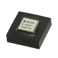
IC ACCEL DIGITAL HI-G 16-LGA
Manufacturer
Analog Devices Inc
Datasheet
1.ADIS16204PCBZ.pdf
(24 pages)
Specifications of ADIS16204BCCZ
Acceleration Range
±37g, 70g
Axis
X, Y
Sensitivity
17.125 LSB/mg, 8.407 LSB/mg
Voltage - Supply
3 V ~ 3.6 V
Output Type
Digital
Bandwidth
400Hz
Interface
SPI
Mounting Type
Surface Mount
Package / Case
16-LGA
No. Of Axes
2
Sensor Case Style
LGA
No. Of Pins
16
Supply Voltage Range
3V To 3.6V
Operating Temperature Range
-40°C To +105°C
Svhc
No SVHC (18-Jun-2010)
Family Name
ADIS16204
Package Type
LGA
Operating Supply Voltage (min)
3V
Operating Supply Voltage (typ)
3.3V
Operating Supply Voltage (max)
3.6V
Operating Temperature (min)
-40C
Operating Temperature (max)
105C
Operating Temperature Classification
Industrial
Product Depth (mm)
8mm
Product Height (mm)
5.2mm
Product Length (mm)
8mm
Mounting
Surface Mount
Pin Count
16
Interface Type
SPI
Sensitivity Per Axis
17.125mg / LSB
Rohs Compliant
Yes
Lead Free Status / RoHS Status
Lead free / RoHS Compliant
For Use With
ADIS16204/PCBZ - BOARD EVAL FOR ADIS16204/PCB
Lead Free Status / Rohs Status
Compliant
Available stocks
Company
Part Number
Manufacturer
Quantity
Price
Company:

Part Number:
ADIS16204BCCZ
Manufacturer:
ST
Quantity:
390


AUXILIARY ADC FUNCTION
The auxiliary ADC function integrates a standard 12-bit ADC
into the ADIS16204 to digitize other system-level analog sig-
nals. The output of the ADC can be monitored through the
AUX_ADC control register, as defined in Table 6. The ADC is
a 12-bit successive approximation converter. The output data
is presented in straight binary format with the full-scale range
extending from 0 V to V
calibrated 2.5 V reference is also provided.
Figure 20 shows the equivalent circuit of the analog input struc-
ture of the ADC. The input capacitor (C1) is typically 4 pF and
can be attributed to parasitic package capacitance. The two diodes
provide ESD protection for the analog input. Care must be
taken to ensure that the analog input signals never exceed the
supply rails by more than 300 mV. This causes the diodes to
become forward-biased and to start conducting. The diodes
can handle 10 mA without causing irreversible damage. The
resistor is a lumped component that represents the on resistance
of the switches. The value of this resistance is typically 100 Ω.
Capacitor C2 represents the ADC sampling capacitor and is
typically 16 pF.
REF
. A high precision, low drift, factory
Rev. B | Page 11 of 24
For ac applications, removing high frequency components from
the analog input signal is recommended by the use of a low-pass
filter on the analog input pin.
In applications where harmonic distortion and signal-to-noise
ratio are critical, the analog input must be driven from a low
impedance source. Large source impedances significantly affect
the ac performance of the ADC. This can necessitate the use of
an input buffer amplifier. When no input amplifier is used to drive
the analog input, the source impedance should be limited to
values lower than 1 kΩ.
Figure 20. Equivalent Analog Input Circuit
Conversion Phase: Switch Open
C1
Track Phase: Switch Closed
VDD
D
D
R1
C2
ADIS16204
Related parts for ADIS16204BCCZ
Image
Part Number
Description
Manufacturer
Datasheet
Request
R

Part Number:
Description:
±1.7g Dual-Axis IMEMS Accelerometer Evaluation Board
Manufacturer:
Analog Devices Inc
Datasheet:

Part Number:
Description:
Inertial Sensor Evaluation System
Manufacturer:
Analog Devices Inc
Datasheet:
Part Number:
Description:
Manufacturer:
Analog Devices Inc
Datasheet:
Part Number:
Description:
Manufacturer:
Analog Devices Inc
Datasheet:
Part Number:
Description:
Manufacturer:
Analog Devices Inc
Datasheet:
Part Number:
Description:
Manufacturer:
Analog Devices Inc
Datasheet:
Part Number:
Description:
Manufacturer:
Analog Devices Inc
Datasheet:
Part Number:
Description:
Manufacturer:
Analog Devices Inc
Datasheet:
Part Number:
Description:
Manufacturer:
Analog Devices Inc
Datasheet:
Part Number:
Description:
Manufacturer:
Analog Devices Inc
Datasheet:
Part Number:
Description:
Manufacturer:
Analog Devices Inc
Datasheet:
Part Number:
Description:
Manufacturer:
Analog Devices Inc
Datasheet:
Part Number:
Description:
Manufacturer:
Analog Devices Inc
Datasheet: