EVAL-ADF70XXEKZ1 Analog Devices Inc, EVAL-ADF70XXEKZ1 Datasheet - Page 5
EVAL-ADF70XXEKZ1
Manufacturer Part Number
EVAL-ADF70XXEKZ1
Description
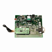
KIT DEV ADF702X FOR BF533EZKIT
Manufacturer
Analog Devices Inc
Type
Transceiver, ISMr
Specifications of EVAL-ADF70XXEKZ1
Frequency
431MHz ~ 464MHz, 862MHz ~ 870MHz, 902MHz ~ 928MHz
For Use With/related Products
ADF702x
For Use With
EVAL-ADF70XXMBZ2 - MOTHER BOARD FOR ADISIMLINK DEV
Lead Free Status / RoHS Status
Lead free / RoHS Compliant


Parameter
CHANNEL FILTERING
BLOCKING
PHASE-LOCKED LOOP
REFERENCE INPUT
TIMING INFORMATION
Adjacent Channel Rejection
Second Adjacent Channel Rejection
Third Adjacent Channel Rejection
Co-Channel Rejection
Wideband Interference Rejection
±1 MHz
±2 MHz
±10 MHz
Saturation (Maximum Input Level)
LNA Input Impedance
RSSI
VCO Gain
Phase Noise (In-Band)
Phase Noise (Out-of-Band)
Residual FM
PLL Settling Time
Crystal Reference
External Oscillator
Load Capacitance
Crystal Start-Up Time
Input Level
Chip Enabled to Regulator Ready
Crystal Oscillator Startup Time
Tx to Rx Turnaround Time
(Offset = ±1 × LP Filter BW Setting)
(Offset = ±2 × LP Filter BW Setting)
(Offset = ±3 × LP Filter BW Setting)
Range at Input
Linearity
Absolute Accuracy
Response Time
Min
3.625
3.625
Typ
27
40
43
−2
42
51
64
12
24 − j60
26 − j63
71 − j128
−100 to
−36
±2
±3
65
83
−89
−110
128
40
33
1
150 µs +
(5 × T
70
150
1.0
10
Rev. A | Page 5 of 44
BIT
)
Max
+24
24
24
Unit
dB
dB
dB
dB
dB
dB
dB
dB
dBm
Ω
Ω
Ω
dBm
dB
dB
µs
MHz/V
MHz/V
dBc/Hz
dBc/Hz
Hz
µs
MHz
MHz
pF
ms
CMOS
µs
ms
levels
Desired signal (38.4 kbps DR, 200 kHz FDEV,
Test Conditions
Desired signal (38.4 kbps DR, 200 kHz FDEV,
Maximum rejection measured with CW
Swept from 100 MHz to 2 GHz,
FSK mode, BER = 10
FRF = 915 MHz, RFIN to GND
FRF = 868 MHz
FRF = 433 MHz
902 MHz to 928 MHz band,
862 MHz to 870 MHz band,
PA = 0 dBm, V
1 MHz offset
From 200 Hz to 20 kHz, FRF = 868MHz
Measured for a 10 MHz frequency step
Using 33 pF load capacitors
C
With 19.2 MHz XTAL
Time to synchronized data,
REG
VCO adjust = 3, VCO_BIAS_SETTING = 12
VCO adjust = 0, VCO_BIAS_SETTING = 10
±300 KHz LP filter B/W) 6 dB above the
input sensitivity level, CW interferer power
level increased until BER = 10
interferer at center of channel
measured as channel rejection
±300 KHz LP filter B/W) 6 dB above the
input sensitivity level, CW interferer power
level increased until BER = 10
FRF = 868 MHz, VCO_BIAS_SETTING = 10
to within 5 ppm accuracy,
PFD = 20 MHz, LBW = 50kHz
includes AGC settling
= 100 nF
DD
= 3.0 V, PFD = 10 MHz,
−3
ADF7025
−3
−3
Related parts for EVAL-ADF70XXEKZ1
Image
Part Number
Description
Manufacturer
Datasheet
Request
R

Part Number:
Description:
IC, ADJ LDO REG, 1.5V TO 5V 250mA MSOP-8
Manufacturer:
Vishay
Datasheet:

Part Number:
Description:
IC, ADJ LDO REG, 1.5V TO 5V 0.6A 8-TSSOP
Manufacturer:
Vishay
Datasheet:
Part Number:
Description:
IC, ADJ LDO REG, 1.5V TO 5V 250mA MSOP-8
Manufacturer:
Vishay
Datasheet:

Part Number:
Description:
IC ADJ LDO REG 1.5V TO 5V 150mA 5-SOT-23
Manufacturer:
Vishay
Datasheet:

Part Number:
Description:
BOARD EVAL AS1324-AD
Manufacturer:
austriamicrosystems
Datasheet:
Part Number:
Description:
IC, ADJ LDO REG, 1.5V TO 5V 0.6A 8-TSSOP
Manufacturer:
Vishay
Datasheet:

Part Number:
Description:
IC, ADJ LDO REG, 1.5V TO 5V, 0.3A, MSOP8
Manufacturer:
Vishay
Datasheet:
Part Number:
Description:
IC, ADJ LDO REG, 1.5V TO 5V, 0.3A, MSOP8
Manufacturer:
Vishay
Datasheet:
Part Number:
Description:
IC, ADJ LDO REG 1.215V TO 5V 0.3A MSOP-8
Manufacturer:
Vishay
Datasheet:
Part Number:
Description:
IC, ADJ LDO REG 1.215V TO 5V 0.3A MSOP-8
Manufacturer:
Vishay
Datasheet:

Part Number:
Description:
±1.7g Dual-Axis IMEMS Accelerometer Evaluation Board
Manufacturer:
Analog Devices Inc
Datasheet:

Part Number:
Description:
IC MULTIPLIER ANALOG 8-SOIC T/R
Manufacturer:
Analog Devices Inc
Datasheet:

Part Number:
Description:
IC ANALOG MULTIPLIER 8-DIP
Manufacturer:
Analog Devices Inc
Datasheet:
Part Number:
Description:
IC ANALOG MULTIPLIER 8-SOIC
Manufacturer:
Analog Devices Inc
Datasheet:
Part Number:
Description:
IC ANALOG MULTIPLIER 8-DIP
Manufacturer:
Analog Devices Inc
Datasheet: