EVAL-ADF70XXEKZ1 Analog Devices Inc, EVAL-ADF70XXEKZ1 Datasheet - Page 25
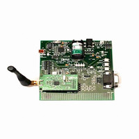
EVAL-ADF70XXEKZ1
Manufacturer Part Number
EVAL-ADF70XXEKZ1
Description
KIT DEV ADF702X FOR BF533EZKIT
Manufacturer
Analog Devices Inc
Type
Transceiver, ISMr
Specifications of EVAL-ADF70XXEKZ1
Frequency
431MHz ~ 464MHz, 862MHz ~ 870MHz, 902MHz ~ 928MHz
For Use With/related Products
ADF702x
For Use With
EVAL-ADF70XXMBZ2 - MOTHER BOARD FOR ADISIMLINK DEV
Lead Free Status / RoHS Status
Lead free / RoHS Compliant


Table 8. Power-Up Sequence Description
Parameter
T
T
T
T
T
T
T
T
0
1
2
6
4
8
9
11
, T
, T
3
7
, T
5
,
19mA TO
3.65mA
2.0mA
22mA
14mA
Value
2 ms
10 µs
32 × 1/SPI_CLK
1 ms
150 µs
5 × bit_period
Packet length
READY
REG.
T
1
WR0
T
2
WR1
T
3
Description/Notes
XTAL starts power-up after CE is brought high. This typically depends on the XTAL
type and the load capacitance specified.
Time for regulator to power up. The serial interface can be written to after this time.
Time to write to a single register. Maximum SPI_CLK is 25 MHz.
The VCO can power-up in parallel with the XTAL. This depends on the CVCO
capacitance value used. A value of 22 nF is recommended as a trade-off
between phase noise performance and power-up time.
This depends on the number of gain changes the AGC loop needs to cycle through
and AGC settings programmed. This is described in more detail in the AGC Information
section.
This is the time for the clock and data recovery circuit to settle. This typically requires
5-bit transitions to acquire sync and is usually covered by the preamble.
Number of bits in payload by the bit period.
XTAL
T
0
VCO
T
4
Figure 36. Rx Programming Sequence and Timing Diagram
WR3
T
5
WR4
T
6
WR6
T
T
7
ON
Rev. A | Page 25 of 44
AGC/
RSSI
T
8
CDR
T
9
Rx
T
DATA
11
T
OFF
TIME
Signal to
Monitor
CLKOUT
CVCO pin
Analog RSSI
on TEST_A pin
MUXOUT
ADF7025
Related parts for EVAL-ADF70XXEKZ1
Image
Part Number
Description
Manufacturer
Datasheet
Request
R

Part Number:
Description:
IC, ADJ LDO REG, 1.5V TO 5V 250mA MSOP-8
Manufacturer:
Vishay
Datasheet:

Part Number:
Description:
IC, ADJ LDO REG, 1.5V TO 5V 0.6A 8-TSSOP
Manufacturer:
Vishay
Datasheet:
Part Number:
Description:
IC, ADJ LDO REG, 1.5V TO 5V 250mA MSOP-8
Manufacturer:
Vishay
Datasheet:

Part Number:
Description:
IC ADJ LDO REG 1.5V TO 5V 150mA 5-SOT-23
Manufacturer:
Vishay
Datasheet:

Part Number:
Description:
BOARD EVAL AS1324-AD
Manufacturer:
austriamicrosystems
Datasheet:
Part Number:
Description:
IC, ADJ LDO REG, 1.5V TO 5V 0.6A 8-TSSOP
Manufacturer:
Vishay
Datasheet:

Part Number:
Description:
IC, ADJ LDO REG, 1.5V TO 5V, 0.3A, MSOP8
Manufacturer:
Vishay
Datasheet:
Part Number:
Description:
IC, ADJ LDO REG, 1.5V TO 5V, 0.3A, MSOP8
Manufacturer:
Vishay
Datasheet:
Part Number:
Description:
IC, ADJ LDO REG 1.215V TO 5V 0.3A MSOP-8
Manufacturer:
Vishay
Datasheet:
Part Number:
Description:
IC, ADJ LDO REG 1.215V TO 5V 0.3A MSOP-8
Manufacturer:
Vishay
Datasheet:

Part Number:
Description:
±1.7g Dual-Axis IMEMS Accelerometer Evaluation Board
Manufacturer:
Analog Devices Inc
Datasheet:

Part Number:
Description:
IC MULTIPLIER ANALOG 8-SOIC T/R
Manufacturer:
Analog Devices Inc
Datasheet:

Part Number:
Description:
IC ANALOG MULTIPLIER 8-DIP
Manufacturer:
Analog Devices Inc
Datasheet:
Part Number:
Description:
IC ANALOG MULTIPLIER 8-SOIC
Manufacturer:
Analog Devices Inc
Datasheet:
Part Number:
Description:
IC ANALOG MULTIPLIER 8-DIP
Manufacturer:
Analog Devices Inc
Datasheet: