EVAL-ADF70XXEKZ1 Analog Devices Inc, EVAL-ADF70XXEKZ1 Datasheet - Page 18
EVAL-ADF70XXEKZ1
Manufacturer Part Number
EVAL-ADF70XXEKZ1
Description
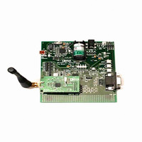
KIT DEV ADF702X FOR BF533EZKIT
Manufacturer
Analog Devices Inc
Type
Transceiver, ISMr
Specifications of EVAL-ADF70XXEKZ1
Frequency
431MHz ~ 464MHz, 862MHz ~ 870MHz, 902MHz ~ 928MHz
For Use With/related Products
ADF702x
For Use With
EVAL-ADF70XXMBZ2 - MOTHER BOARD FOR ADISIMLINK DEV
Lead Free Status / RoHS Status
Lead free / RoHS Compliant


ADF7025
TRANSMITTER
RF OUTPUT STAGE
The PA of the ADF7025 is based on a single-ended, controlled
current, open-drain amplifier that has been designed to deliver
up to 13 dBm into a 50 Ω load at a maximum frequency of
928 MHz.
The PA output current and, consequently, the output power are
programmable over a wide range. The PA configuration is
shown in Figure 25. The output power is independent of the
state of the DATA I/O pin. The output power is set using Bits
R2_DB [9:14].
The PA is equipped with overvoltage protection, which makes it
robust in severe mismatch conditions. Depending on the
application, one can design a matching network for the PA to
exhibit optimum efficiency at the desired radiated output power
level for a wide range of different antennas, such as loop or
monopole antennas. See the LNA/PA Matching section for
details.
PA Bias Currents
Control Bits R2_DB [30:31] facilitate an adjustment of the PA
bias current to further extend the output power control range, if
necessary. If this feature is not required, the default value of
7 µA is recommended. The output stage is powered down by
resetting Bit R2_DB4.
RFGND
RFOUT
FROM VCO
+
Figure 25. PA Configuration
R2_DB(30:31)
IDAC
2
6
R2_DB(9:14)
R2_DB4
R2_DB5
DIGITAL
LOCK DETECT
Rev. A | Page 18 of 44
MODULATION SCHEME
Frequency Shift Keying (FSK)
Frequency shift keying is implemented by setting the N value for
the center frequency and then toggling this with the TxData
line. The deviation from the center frequency is set using
Bits R2_DB [15:23]. The deviation from the center frequency in
Hz is
where Modulation Number is a number from 1 to 511
(R2_DB(15:23)).
Select FSK using Bits R2_DB [6:8].
The choice of deviation frequency for a given data rate is critical
to get optimum sensitivity performance from the ADF7025.
The modulation index (MI) of an FSK modulated signal is
defined as
It is recommended to use a MI > 1 for the ADF7025. The
variation of receiver sensitivity with modulation index, for
various data rates, can be observed in Figure 16, Figure 17,
and Figure 18.
Modulation Index
FSK DEVIATION
TxDATA
FREQUENCY
+F
–F
FSK
MI
DEV
DEV
=
DEVIATION
2
4R
×
Frequency
Data
[Hz]
CHARGE
FRACTIONAL-N
Figure 26. FSK Implementation
PUMP
PFD/
=
Rate
PFD
Deviation
[bps]
Σ-∆ MODULATOR
THIRD-ORDER
×
Modulation
[Hz]
2
14
INTEGER-N
Number
VCO
÷N
PA STAGE
Related parts for EVAL-ADF70XXEKZ1
Image
Part Number
Description
Manufacturer
Datasheet
Request
R

Part Number:
Description:
IC, ADJ LDO REG, 1.5V TO 5V 250mA MSOP-8
Manufacturer:
Vishay
Datasheet:

Part Number:
Description:
IC, ADJ LDO REG, 1.5V TO 5V 0.6A 8-TSSOP
Manufacturer:
Vishay
Datasheet:
Part Number:
Description:
IC, ADJ LDO REG, 1.5V TO 5V 250mA MSOP-8
Manufacturer:
Vishay
Datasheet:

Part Number:
Description:
IC ADJ LDO REG 1.5V TO 5V 150mA 5-SOT-23
Manufacturer:
Vishay
Datasheet:

Part Number:
Description:
BOARD EVAL AS1324-AD
Manufacturer:
austriamicrosystems
Datasheet:
Part Number:
Description:
IC, ADJ LDO REG, 1.5V TO 5V 0.6A 8-TSSOP
Manufacturer:
Vishay
Datasheet:

Part Number:
Description:
IC, ADJ LDO REG, 1.5V TO 5V, 0.3A, MSOP8
Manufacturer:
Vishay
Datasheet:
Part Number:
Description:
IC, ADJ LDO REG, 1.5V TO 5V, 0.3A, MSOP8
Manufacturer:
Vishay
Datasheet:
Part Number:
Description:
IC, ADJ LDO REG 1.215V TO 5V 0.3A MSOP-8
Manufacturer:
Vishay
Datasheet:
Part Number:
Description:
IC, ADJ LDO REG 1.215V TO 5V 0.3A MSOP-8
Manufacturer:
Vishay
Datasheet:

Part Number:
Description:
±1.7g Dual-Axis IMEMS Accelerometer Evaluation Board
Manufacturer:
Analog Devices Inc
Datasheet:

Part Number:
Description:
IC MULTIPLIER ANALOG 8-SOIC T/R
Manufacturer:
Analog Devices Inc
Datasheet:

Part Number:
Description:
IC ANALOG MULTIPLIER 8-DIP
Manufacturer:
Analog Devices Inc
Datasheet:
Part Number:
Description:
IC ANALOG MULTIPLIER 8-SOIC
Manufacturer:
Analog Devices Inc
Datasheet:
Part Number:
Description:
IC ANALOG MULTIPLIER 8-DIP
Manufacturer:
Analog Devices Inc
Datasheet: