EVAL-ADF70XXEKZ1 Analog Devices Inc, EVAL-ADF70XXEKZ1 Datasheet - Page 19
EVAL-ADF70XXEKZ1
Manufacturer Part Number
EVAL-ADF70XXEKZ1
Description
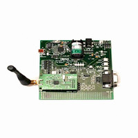
KIT DEV ADF702X FOR BF533EZKIT
Manufacturer
Analog Devices Inc
Type
Transceiver, ISMr
Specifications of EVAL-ADF70XXEKZ1
Frequency
431MHz ~ 464MHz, 862MHz ~ 870MHz, 902MHz ~ 928MHz
For Use With/related Products
ADF702x
For Use With
EVAL-ADF70XXMBZ2 - MOTHER BOARD FOR ADISIMLINK DEV
Lead Free Status / RoHS Status
Lead free / RoHS Compliant


Tx/Rx SELECT
RECEIVER
RF FRONT END
The ADF7025 is based on a fully integrated, zero-IF receiver
architecture. The zero-IF architecture minimizes power
consumption and the external component count while avoiding
the need for image rejection.
Figure 27 shows the structure of the receiver front end. The
numerous programming options allow users to trade off
sensitivity, linearity, and current consumption against each
other in the way best suitable for their applications. To achieve a
high level of resilience against spurious reception, the LNA
features a differential input. Switch SW2 shorts the LNA input
when transmit mode is selected (R0_DB27 = 0). This feature
facilitates the design of a combined LNA/PA matching network,
avoiding the need for an external Rx/Tx switch. See the
LNA/PA Matching section for details on the design of the
matching network.
The LNA is followed by a quadrature downconversion mixer,
which converts the RF signal direct to baseband. The output
frequency of the synthesizer must be programmed to the value
equal to the center frequency of the received channel.
The LNA has two basic operating modes: high gain/low noise
mode and low gain/low power mode. To switch between the
two modes, use the LNA_mode bit, R6_DB15. The mixer is also
configurable between a low current and an enhanced linearity
mode using the mixer_linearity bit, R6_DB18.
LNA/MIXER ENABLE
[R0_DB27]
LNA CURRENT
[R6_DB(16:17)]
[R9_DB(20:21)]
RFINB
LNA MODE
[R6_DB15]
RFIN
LNA GAIN
[R8_DB6]
Figure 27. ADF7025 RF Front End
SW2
LNA
LO
I (TO FILTER)
Q (TO FILTER)
MIXER LINEARITY
[R6_DB18]
Rev. A | Page 19 of 44
Based on the specific sensitivity and linearity requirements of
the application, it is recommended to adjust control bits
LNA_mode (R6_DB15) and mixer_linearity (R6_DB18).
The gain of the LNA is configured by the LNA_gain field,
R9_DB [20:21] and can be set by either the user or the
automatic gain control (AGC) logic.
Filter Settings/Calibration
Out-of-band interference is rejected by means of a fifth-order,
low-pass filter (LPF). The bandwidth of the filter can be
programmed to be ±300 kHz, ±450 kHz, or ±600 kHz by means
of Control Bits R1_DB [22:23] and should be chosen as a
compromise between interference rejection and attenuation of
the desired signal. A high-pass filter is also included as part of
the low-pass filter to prevent against dc offset problems. The
bandwidth of this filter is ~60 kHz. To avoid significant loss of
FSK modulated signal in the filter, the frequency deviation
needs to be significantly larger than this pole (refer to the
Modulation Index section). The minimum allowable frequency
deviation is 100 kHz.
To compensate for manufacturing tolerances, the LPF should
be calibrated once after power-up. The LPF calibration logic
requires that the LPF divider in Bits R6_DB [20:28] be set
depending on the crystal frequency. Once initiated by setting
Bit R6_DB19, the calibration is performed automatically
without any user intervention. The calibration time is 200 µs,
during which the ADF7025 should not be accessed. It is
important not to initiate the calibration cycle before the crystal
oscillator has fully settled. If the AGC loop is disabled, the gain
of LPF can be set to three levels using the filter_gain field,
R9_DB [20:21]. The filter gain is adjusted automatically, if the
AGC loop is enabled.
ADF7025
Related parts for EVAL-ADF70XXEKZ1
Image
Part Number
Description
Manufacturer
Datasheet
Request
R

Part Number:
Description:
IC, ADJ LDO REG, 1.5V TO 5V 250mA MSOP-8
Manufacturer:
Vishay
Datasheet:

Part Number:
Description:
IC, ADJ LDO REG, 1.5V TO 5V 0.6A 8-TSSOP
Manufacturer:
Vishay
Datasheet:
Part Number:
Description:
IC, ADJ LDO REG, 1.5V TO 5V 250mA MSOP-8
Manufacturer:
Vishay
Datasheet:

Part Number:
Description:
IC ADJ LDO REG 1.5V TO 5V 150mA 5-SOT-23
Manufacturer:
Vishay
Datasheet:

Part Number:
Description:
BOARD EVAL AS1324-AD
Manufacturer:
austriamicrosystems
Datasheet:
Part Number:
Description:
IC, ADJ LDO REG, 1.5V TO 5V 0.6A 8-TSSOP
Manufacturer:
Vishay
Datasheet:

Part Number:
Description:
IC, ADJ LDO REG, 1.5V TO 5V, 0.3A, MSOP8
Manufacturer:
Vishay
Datasheet:
Part Number:
Description:
IC, ADJ LDO REG, 1.5V TO 5V, 0.3A, MSOP8
Manufacturer:
Vishay
Datasheet:
Part Number:
Description:
IC, ADJ LDO REG 1.215V TO 5V 0.3A MSOP-8
Manufacturer:
Vishay
Datasheet:
Part Number:
Description:
IC, ADJ LDO REG 1.215V TO 5V 0.3A MSOP-8
Manufacturer:
Vishay
Datasheet:

Part Number:
Description:
±1.7g Dual-Axis IMEMS Accelerometer Evaluation Board
Manufacturer:
Analog Devices Inc
Datasheet:

Part Number:
Description:
IC MULTIPLIER ANALOG 8-SOIC T/R
Manufacturer:
Analog Devices Inc
Datasheet:

Part Number:
Description:
IC ANALOG MULTIPLIER 8-DIP
Manufacturer:
Analog Devices Inc
Datasheet:
Part Number:
Description:
IC ANALOG MULTIPLIER 8-SOIC
Manufacturer:
Analog Devices Inc
Datasheet:
Part Number:
Description:
IC ANALOG MULTIPLIER 8-DIP
Manufacturer:
Analog Devices Inc
Datasheet: