EVAL-ADF70XXEKZ1 Analog Devices Inc, EVAL-ADF70XXEKZ1 Datasheet - Page 24
EVAL-ADF70XXEKZ1
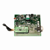
Manufacturer Part Number
EVAL-ADF70XXEKZ1
Description
KIT DEV ADF702X FOR BF533EZKIT
Manufacturer
Analog Devices Inc
Type
Transceiver, ISMr
Specifications of EVAL-ADF70XXEKZ1
Frequency
431MHz ~ 464MHz, 862MHz ~ 870MHz, 902MHz ~ 928MHz
For Use With/related Products
ADF702x
For Use With
EVAL-ADF70XXMBZ2 - MOTHER BOARD FOR ADISIMLINK DEV
Lead Free Status / RoHS Status
Lead free / RoHS Compliant


ADF7025
The procedure typically requires several iterations until an
acceptable compromise is reached. The successful implementation
of a combined LNA/PA matching network for the ADF7025 is
critically dependent on the availability of an accurate electrical
model for the PC board. In this context, the use of a suitable CAD
package is strongly recommended. To avoid this effort, however, a
small form-factor reference design for the ADF7025 is provided,
including matching and harmonic filter components. The design
is on a 2-layer PCB to minimize cost. Gerber files are available
on the
TRANSMIT PROTOCOL AND CODING
CONSIDERATIONS
A dc-free preamble pattern is recommended for FSK
demodulation. The recommended preamble pattern is a dc-free
pattern such as a 10101010… pattern. Preamble patterns with
longer run-length constraints such as 11001100…. can also be
used. However, this results in a longer synchronization time of
the received bit stream in the receiver.
Manchester coding can be used for the entire transmit protocol.
However, the remaining fields that follow the preamble header
do not have to use dc-free coding. For these fields, the ADF7025
can accommodate coding schemes with a run-length of up to
six bits without any performance degradation.
If longer run-length coding must be supported, the ADF7025
has several other features that can be activated. These involve a
range of programmable options that allow the envelope detector
output to be frozen after preamble acquisition.
DEVICE PROGRAMMING AFTER INITIAL POWER-UP
Table 7 lists the minimum number of writes needed to set up
the ADF7025 in either Tx or Rx mode after CE is brought high.
Additional registers can also be written to tailor the part to a
particular application, such as setting up sync byte detection.
When going from Tx to Rx or vice versa, the user needs to write
only to the N register to alter the LO by 200 kHz and to toggle
the Tx/Rx bit.
PREAMBLE
www.analog.com
Figure 33. Typical Format of a Transmit Protocol
WORD
SYNC
website.
FIELD
ID
DATA FIELD
CRC
Rev. A | Page 24 of 44
1
Table 7. Minimum Register Writes Required for Tx/Rx Setup
Mode
Tx
Rx (FSK)
Tx to Rx and Rx to Tx
Figure 36 and Figure 37 show the recommended programming
sequence and associated timing for power-up from standby
mode.
INTERFACING TO MICROCONTROLLER/DSP
Low level device drivers are available for interfacing to the
ADF7025, the ADI ADuC84x microcontroller parts, or the
Blackfin® BF53x DSPs using the hardware connections shown in
Figure 34 and Figure 35.
Register 9 should be programmed in receive mode in order to set the
recommended AGC threshold settings (low = 15, high = 79).
ADSP-BF533
ADuC84x
GPIO
RSCLK1
P3.2/INT0
DR1PRI
Figure 34. ADuC84X to ADF7025 Connection Diagram
DT1PRI
SCLOCK
MOSI
MISO
RFS1
Figure 35. BF533 to ADF7025 Connection Diagram
GND
SCK
VCC
PF5
PF6
MISO
MOSI
P3.7
P2.4
P2.5
P2.6
P2.7
SS
Registers
0
0
0
1
1
2
2
SCLK
SDATA
SREAD
SLE
TxRxCLK
TxRxDATA
INT/LOCK
CE
VCC
GND
ADF7025
TxRxDATA
RxCLK
CE
INT/LOCK
SREAD
SLE
SDATA
SCLK
4
ADF7025
6
9
1
Related parts for EVAL-ADF70XXEKZ1
Image
Part Number
Description
Manufacturer
Datasheet
Request
R

Part Number:
Description:
IC, ADJ LDO REG, 1.5V TO 5V 250mA MSOP-8
Manufacturer:
Vishay
Datasheet:

Part Number:
Description:
IC, ADJ LDO REG, 1.5V TO 5V 0.6A 8-TSSOP
Manufacturer:
Vishay
Datasheet:
Part Number:
Description:
IC, ADJ LDO REG, 1.5V TO 5V 250mA MSOP-8
Manufacturer:
Vishay
Datasheet:

Part Number:
Description:
IC ADJ LDO REG 1.5V TO 5V 150mA 5-SOT-23
Manufacturer:
Vishay
Datasheet:

Part Number:
Description:
BOARD EVAL AS1324-AD
Manufacturer:
austriamicrosystems
Datasheet:
Part Number:
Description:
IC, ADJ LDO REG, 1.5V TO 5V 0.6A 8-TSSOP
Manufacturer:
Vishay
Datasheet:

Part Number:
Description:
IC, ADJ LDO REG, 1.5V TO 5V, 0.3A, MSOP8
Manufacturer:
Vishay
Datasheet:
Part Number:
Description:
IC, ADJ LDO REG, 1.5V TO 5V, 0.3A, MSOP8
Manufacturer:
Vishay
Datasheet:
Part Number:
Description:
IC, ADJ LDO REG 1.215V TO 5V 0.3A MSOP-8
Manufacturer:
Vishay
Datasheet:
Part Number:
Description:
IC, ADJ LDO REG 1.215V TO 5V 0.3A MSOP-8
Manufacturer:
Vishay
Datasheet:

Part Number:
Description:
±1.7g Dual-Axis IMEMS Accelerometer Evaluation Board
Manufacturer:
Analog Devices Inc
Datasheet:

Part Number:
Description:
IC MULTIPLIER ANALOG 8-SOIC T/R
Manufacturer:
Analog Devices Inc
Datasheet:

Part Number:
Description:
IC ANALOG MULTIPLIER 8-DIP
Manufacturer:
Analog Devices Inc
Datasheet:
Part Number:
Description:
IC ANALOG MULTIPLIER 8-SOIC
Manufacturer:
Analog Devices Inc
Datasheet:
Part Number:
Description:
IC ANALOG MULTIPLIER 8-DIP
Manufacturer:
Analog Devices Inc
Datasheet: