DK-DEV-5M570ZN Altera, DK-DEV-5M570ZN Datasheet - Page 7
DK-DEV-5M570ZN
Manufacturer Part Number
DK-DEV-5M570ZN
Description
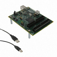
KIT DEV MAX V 5M570Z
Manufacturer
Altera
Series
MAX® Vr
Type
CPLDr
Datasheets
1.DK-DEV-5M570ZN.pdf
(30 pages)
2.DK-DEV-5M570ZN.pdf
(2 pages)
3.DK-DEV-5M570ZN.pdf
(30 pages)
4.DK-DEV-5M570ZN.pdf
(164 pages)
5.DK-DEV-5M570ZN.pdf
(24 pages)
Specifications of DK-DEV-5M570ZN
Contents
Board, Cable(s), Software and Documentation
Silicon Manufacturer
Altera
Core Architecture
CPLD
Core Sub-architecture
MAX
Silicon Core Number
5M
Silicon Family Name
MAX V
Kit Contents
MAX V CPLD Development Board, USB Cable
Rohs Compliant
Yes
Lead Free Status / RoHS Status
Lead free / RoHS Compliant
For Use With/related Products
5M570ZF256
Lead Free Status / Rohs Status
Compliant
Other names
544-2722
Available stocks
Company
Part Number
Manufacturer
Quantity
Price


Chapter 3: DC and Switching Characteristics for MAX V Devices
Operating Conditions
Table 3–9. 1.5-V I/O Specifications for MAX V Devices
Table 3–10. 1.2-V I/O Specifications for MAX V Devices
Table 3–11. 3.3-V PCI Specifications for MAX V Devices
Table 3–12. LVDS Specifications for MAX V Devices
January 2011 Altera Corporation
V
V
V
V
V
Notes to
(1) This specification is supported across all the programmable drive strength settings available for this I/O standard, as shown in the
(2) This maximum V
V
V
V
V
V
Note to
(1) This specification is supported across all the programmable drive strength settings available for this I/O standard, as shown in the
V
V
V
V
V
Note to
(1) 3.3-V PCI I/O standard is only supported in Bank 3 of the 5M1270Z and 5M2210Z devices.
V
V
V
Note to
(1) Supports emulated LVDS output using a three-resistor network (LVDS_E_3R).
CCIO
IH
IL
OH
OL
CCIO
IH
IL
OH
OL
CCIO
IH
IL
OH
OL
CCIO
OD
OS
Symbol
Symbol
Symbol
Symbol
MAX V Device Architecture
in
MAX V Device Architecture
Table 3–2 on page
Table
Table
Table
Table
3–10:
3–11:
3–12:
3–9:
I/O supply voltage
Differential output voltage swing
Output offset voltage
I/O supply voltage
High-level input voltage
Low-level input voltage
High-level output voltage
Low-level output voltage
I/O supply voltage
High-level input voltage
Low-level input voltage
High-level output voltage
Low-level output voltage
I/O supply voltage
High-level input voltage
Low-level input voltage
High-level output voltage
Low-level output voltage
IH
reflects the JEDEC specification. The MAX V input buffer can tolerate a V
3–2.
Parameter
chapter.
chapter.
Parameter
Parameter
Parameter
IOH = –2 mA
IOH = –2 mA
IOH = –500 µA
IOL = 2 mA
IOL = 2 mA
IOL = 1.5 mA
(Note 1)
Conditions
Conditions
Conditions
Conditions
(Note 1)
—
—
—
—
—
—
—
—
—
—
—
—
(1)
(1)
(1)
(1)
0.5 × V
0.9 × V
Minimum
Minimum
2.375
1.125
–0.5
0.65 × V
0.75 × V
0.75 × V
3.0
247
—
0.8 × V
Minimum
Minimum
1.425
IH
CCIO
CCIO
–0.3
1.14
–0.3
—
maximum of 4.0, as specified by the V
—
CCIO
CCIO
CCIO
CCIO
Typical
Typical
1.25
3.3
—
—
—
—
2.5
—
V
CCIO
0.35 × V
0.25 × V
0.25 × V
0.25 × V
V
Maximum
Maximum
CCIO
1.575
1.26
+ 0.3
—
—
V
0.3 × V
0.1 × V
Maximum
Maximum
MAX V Device Handbook
+ 0.3
CCIO
2.625
1.375
CCIO
CCIO
CCIO
CCIO
3.6
600
—
(2)
+ 0.5
CCIO
CCIO
I
parameter
Unit
Unit
V
V
V
V
V
V
V
V
V
V
Unit
Unit
mV
V
V
V
V
V
V
V
3–7
Related parts for DK-DEV-5M570ZN
Image
Part Number
Description
Manufacturer
Datasheet
Request
R

Part Number:
Description:
KIT DEV ARRIA II GX FPGA 2AGX125
Manufacturer:
Altera
Datasheet:

Part Number:
Description:
KIT DEV CYCLONE III LS EP3CLS200
Manufacturer:
Altera
Datasheet:

Part Number:
Description:
KIT DEV STRATIX IV FPGA 4SE530
Manufacturer:
Altera
Datasheet:

Part Number:
Description:
KIT DEV FPGA 2AGX260 W/6.375G TX
Manufacturer:
Altera
Datasheet:

Part Number:
Description:
KIT DEV STRATIX V FPGA 5SGXEA7
Manufacturer:
Altera
Datasheet:

Part Number:
Description:
KIT DEVELOPMENT STRATIX III
Manufacturer:
Altera
Datasheet:

Part Number:
Description:
KIT DEVELOPMENT STRATIX IV
Manufacturer:
Altera
Datasheet:

Part Number:
Description:
KIT DEV ARRIA GX 1AGX60N
Manufacturer:
Altera
Datasheet:
Part Number:
Description:
KIT STARTER CYCLONE IV GX
Manufacturer:
Altera
Datasheet:
Part Number:
Description:
KIT DEVELOPMENT STRATIX IV
Manufacturer:
Altera
Datasheet:

Part Number:
Description:
CPLD, EP610 Family, ECMOS Process, 300 Gates, 16 Macro Cells, 16 Reg., 16 User I/Os, 5V Supply, 35 Speed Grade, 24DIP
Manufacturer:
Altera Corporation
Datasheet:
Part Number:
Description:
CPLD, EP610 Family, ECMOS Process, 300 Gates, 16 Macro Cells, 16 Reg., 16 User I/Os, 5V Supply, 15 Speed Grade, 24DIP
Manufacturer:
Altera Corporation
Datasheet: