DK-DEV-5M570ZN Altera, DK-DEV-5M570ZN Datasheet - Page 10
DK-DEV-5M570ZN
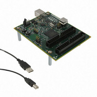
Manufacturer Part Number
DK-DEV-5M570ZN
Description
KIT DEV MAX V 5M570Z
Manufacturer
Altera
Series
MAX® Vr
Type
CPLDr
Datasheets
1.DK-DEV-5M570ZN.pdf
(30 pages)
2.DK-DEV-5M570ZN.pdf
(2 pages)
3.DK-DEV-5M570ZN.pdf
(30 pages)
4.DK-DEV-5M570ZN.pdf
(164 pages)
5.DK-DEV-5M570ZN.pdf
(24 pages)
Specifications of DK-DEV-5M570ZN
Contents
Board, Cable(s), Software and Documentation
Silicon Manufacturer
Altera
Core Architecture
CPLD
Core Sub-architecture
MAX
Silicon Core Number
5M
Silicon Family Name
MAX V
Kit Contents
MAX V CPLD Development Board, USB Cable
Rohs Compliant
Yes
Lead Free Status / RoHS Status
Lead free / RoHS Compliant
For Use With/related Products
5M570ZF256
Lead Free Status / Rohs Status
Compliant
Other names
544-2722
Available stocks
Company
Part Number
Manufacturer
Quantity
Price


3–10
Timing Model and Specifications
Figure 3–2. Timing Model for MAX V Devices
MAX V Device Handbook
I/O Pin
Preliminary and Final Timing
INPUT
I/O Input Delay
f
t
IN
MAX V devices timing can be analyzed with the Altera Quartus
of industry-standard EDA simulators and timing analyzers, or with the timing model
shown in
MAX V devices have predictable internal delays that allow you to determine the
worst-case timing of any design. The software provides timing simulation,
point-to-point delay prediction, and detailed timing analysis for device-wide
performance evaluation.
You can derive the timing characteristics of any signal path from the timing model
and parameters of a particular device. You can calculate external timing parameters,
which represent pin-to-pin timing delays, as the sum of the internal parameters.
For more information, refer to
This section describes the performance, internal, external, and UFM timing
specifications. All specifications are representative of the worst-case supply voltage
and junction temperature conditions.
Timing models can have either preliminary or final status. The Quartus II software
issues an informational message during the design compilation if the timing models
are preliminary.
Preliminary status means the timing model is subject to change. Initially, timing
numbers are created using simulation results, process data, and other known
parameters. These tests are used to make the preliminary numbers as close to the
actual timing parameters as possible.
Input Routing
Global Input Delay
Memory
Delay
Flash
User
t
DL
t
GLOB
Figure
Data-In/LUT Chain
Table 3–16
3–2.
To Adjacent LE
Register Control
LUT Delay
t
Logic Element
Delay
LUT
t
C
t
R4
lists the status of the MAX V device timing models.
AN629: Understanding Timing in Altera
t
COMB
t
t
t
t
PRE
CLR
CO
SU
t
H
Register Delays
Chapter 3: DC and Switching Characteristics for MAX V Devices
t
C4
Data-Out
Combinational Path Delay
From Adjacent LE
Output Routing
t
Delay
FASTIO
t
IODR
t
IOE
January 2011 Altera Corporation
Output and Output Enable
Timing Model and Specifications
®
II software, a variety
Data Delay
Output
Delay
t
t
t
OD
XZ
ZX
CPLDs.
I/O Pin
Related parts for DK-DEV-5M570ZN
Image
Part Number
Description
Manufacturer
Datasheet
Request
R

Part Number:
Description:
KIT DEV ARRIA II GX FPGA 2AGX125
Manufacturer:
Altera
Datasheet:

Part Number:
Description:
KIT DEV CYCLONE III LS EP3CLS200
Manufacturer:
Altera
Datasheet:

Part Number:
Description:
KIT DEV STRATIX IV FPGA 4SE530
Manufacturer:
Altera
Datasheet:

Part Number:
Description:
KIT DEV FPGA 2AGX260 W/6.375G TX
Manufacturer:
Altera
Datasheet:

Part Number:
Description:
KIT DEV STRATIX V FPGA 5SGXEA7
Manufacturer:
Altera
Datasheet:

Part Number:
Description:
KIT DEVELOPMENT STRATIX III
Manufacturer:
Altera
Datasheet:

Part Number:
Description:
KIT DEVELOPMENT STRATIX IV
Manufacturer:
Altera
Datasheet:

Part Number:
Description:
KIT DEV ARRIA GX 1AGX60N
Manufacturer:
Altera
Datasheet:
Part Number:
Description:
KIT STARTER CYCLONE IV GX
Manufacturer:
Altera
Datasheet:
Part Number:
Description:
KIT DEVELOPMENT STRATIX IV
Manufacturer:
Altera
Datasheet:

Part Number:
Description:
CPLD, EP610 Family, ECMOS Process, 300 Gates, 16 Macro Cells, 16 Reg., 16 User I/Os, 5V Supply, 35 Speed Grade, 24DIP
Manufacturer:
Altera Corporation
Datasheet:
Part Number:
Description:
CPLD, EP610 Family, ECMOS Process, 300 Gates, 16 Macro Cells, 16 Reg., 16 User I/Os, 5V Supply, 15 Speed Grade, 24DIP
Manufacturer:
Altera Corporation
Datasheet: