DK-DEV-5M570ZN Altera, DK-DEV-5M570ZN Datasheet - Page 21
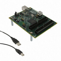
DK-DEV-5M570ZN
Manufacturer Part Number
DK-DEV-5M570ZN
Description
KIT DEV MAX V 5M570Z
Manufacturer
Altera
Series
MAX® Vr
Type
CPLDr
Datasheets
1.DK-DEV-5M570ZN.pdf
(30 pages)
2.DK-DEV-5M570ZN.pdf
(2 pages)
3.DK-DEV-5M570ZN.pdf
(30 pages)
4.DK-DEV-5M570ZN.pdf
(164 pages)
5.DK-DEV-5M570ZN.pdf
(24 pages)
Specifications of DK-DEV-5M570ZN
Contents
Board, Cable(s), Software and Documentation
Silicon Manufacturer
Altera
Core Architecture
CPLD
Core Sub-architecture
MAX
Silicon Core Number
5M
Silicon Family Name
MAX V
Kit Contents
MAX V CPLD Development Board, USB Cable
Rohs Compliant
Yes
Lead Free Status / RoHS Status
Lead free / RoHS Compliant
For Use With/related Products
5M570ZF256
Lead Free Status / Rohs Status
Compliant
Other names
544-2722
Available stocks
Company
Part Number
Manufacturer
Quantity
Price


Chapter 3: DC and Switching Characteristics for MAX V Devices
Timing Model and Specifications
Table 3–29. Global Clock External I/O Timing Parameters for the 5M1270Z Device
Table 3–30. Global Clock External I/O Timing Parameters for the 5M1270Z Device
Table 3–31. Global Clock External I/O Timing Parameters for the 5M2210Z Device
January 2011 Altera Corporation
t
t
f
Notes to
(1) The maximum frequency is limited by the I/O standard on the clock input pin. The 16-bit counter critical delay performs faster than this global
(2) Not applicable to the F324 package of the 5M1270Z device.
t
t
t
t
t
t
t
t
f
Notes to
(1) The maximum frequency is limited by the I/O standard on the clock input pin. The 16-bit counter critical delay performs faster than this global
(2) Only applicable to the F324 package of the 5M1270Z device.
t
t
t
t
CL
CNT
CNT
PD1
PD2
SU
H
CO
CH
CL
CNT
CNT
PD1
PD2
SU
H
Symbol
Symbol
Symbol
clock input pin maximum frequency.
clock input pin maximum frequency.
Table
Table
Global clock low time
Minimum global clock period for 16-bit
counter
Maximum global clock frequency for 16-bit
counter
Worst case pin-to-pin delay through one LUT
Best case pin-to-pin delay through one LUT
Global clock setup time
Global clock hold time
Global clock to output delay
Global clock high time
Global clock low time
Minimum global clock period for 16-bit
counter
Maximum global clock frequency for 16-bit
counter
Worst case pin-to-pin delay through one LUT
Best case pin-to-pin delay through one LUT
Global clock setup time
Global clock hold time
3–29:
3–30:
Table 3–30
5M1270Z device.
Table 3–31
Parameter
Parameter
Parameter
lists the external I/O timing parameters for the F324 package of the
lists the external I/O timing parameters for the 5M2210Z device.
Condition
Condition
Condition
10 pF
10 pF
10 pF
10 pF
10 pF
—
—
—
—
—
—
—
—
—
—
—
Min
216
Min
216
Min
216
2.0
4.0
1.5
4.0
1.5
—
—
—
—
—
—
0
0
C4
C4
C4
(Note
(Note
(Note 1)
247.5
247.5
Max
Max
Max
9.1
4.8
6.0
9.1
4.8
—
—
—
—
—
—
—
—
—
1),
1),
(Part 1 of 2)
(2)
(2)
Min
Min
Min
266
266
266
5.0
1.9
2.0
5.0
1.9
—
—
—
—
—
—
(Part 2 of 2)
0
0
C5, I5
C5, I5
C5, I5
MAX V Device Handbook
201.1
201.1
Max
Max
11.2
Max
11.2
5.9
7.4
5.9
—
—
—
—
—
—
—
—
—
MHz
MHz
Unit
Unit
Unit
3–21
ps
ns
ns
ns
ns
ns
ns
ps
ps
ns
ns
ns
ns
ns
Related parts for DK-DEV-5M570ZN
Image
Part Number
Description
Manufacturer
Datasheet
Request
R

Part Number:
Description:
KIT DEV ARRIA II GX FPGA 2AGX125
Manufacturer:
Altera
Datasheet:

Part Number:
Description:
KIT DEV CYCLONE III LS EP3CLS200
Manufacturer:
Altera
Datasheet:

Part Number:
Description:
KIT DEV STRATIX IV FPGA 4SE530
Manufacturer:
Altera
Datasheet:

Part Number:
Description:
KIT DEV FPGA 2AGX260 W/6.375G TX
Manufacturer:
Altera
Datasheet:

Part Number:
Description:
KIT DEV STRATIX V FPGA 5SGXEA7
Manufacturer:
Altera
Datasheet:

Part Number:
Description:
KIT DEVELOPMENT STRATIX III
Manufacturer:
Altera
Datasheet:

Part Number:
Description:
KIT DEVELOPMENT STRATIX IV
Manufacturer:
Altera
Datasheet:

Part Number:
Description:
KIT DEV ARRIA GX 1AGX60N
Manufacturer:
Altera
Datasheet:
Part Number:
Description:
KIT STARTER CYCLONE IV GX
Manufacturer:
Altera
Datasheet:
Part Number:
Description:
KIT DEVELOPMENT STRATIX IV
Manufacturer:
Altera
Datasheet:

Part Number:
Description:
CPLD, EP610 Family, ECMOS Process, 300 Gates, 16 Macro Cells, 16 Reg., 16 User I/Os, 5V Supply, 35 Speed Grade, 24DIP
Manufacturer:
Altera Corporation
Datasheet:
Part Number:
Description:
CPLD, EP610 Family, ECMOS Process, 300 Gates, 16 Macro Cells, 16 Reg., 16 User I/Os, 5V Supply, 15 Speed Grade, 24DIP
Manufacturer:
Altera Corporation
Datasheet: