DK-DEV-5M570ZN Altera, DK-DEV-5M570ZN Datasheet - Page 4
DK-DEV-5M570ZN
Manufacturer Part Number
DK-DEV-5M570ZN
Description
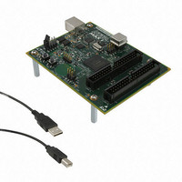
KIT DEV MAX V 5M570Z
Manufacturer
Altera
Series
MAX® Vr
Type
CPLDr
Datasheets
1.DK-DEV-5M570ZN.pdf
(30 pages)
2.DK-DEV-5M570ZN.pdf
(2 pages)
3.DK-DEV-5M570ZN.pdf
(30 pages)
4.DK-DEV-5M570ZN.pdf
(164 pages)
5.DK-DEV-5M570ZN.pdf
(24 pages)
Specifications of DK-DEV-5M570ZN
Contents
Board, Cable(s), Software and Documentation
Silicon Manufacturer
Altera
Core Architecture
CPLD
Core Sub-architecture
MAX
Silicon Core Number
5M
Silicon Family Name
MAX V
Kit Contents
MAX V CPLD Development Board, USB Cable
Rohs Compliant
Yes
Lead Free Status / RoHS Status
Lead free / RoHS Compliant
For Use With/related Products
5M570ZF256
Lead Free Status / Rohs Status
Compliant
Other names
544-2722
Available stocks
Company
Part Number
Manufacturer
Quantity
Price


3–4
Table 3–4. DC Electrical Characteristics for MAX V Devices
MAX V Device Handbook
I
C
C
Notes to
(1) Typical values are for T
(2) This value is specified for normal device operation. The value may vary during power-up. This applies to all V
(3) V
(4) Commercial temperature ranges from 0°C to 85°C with the maximum current at 85°C.
(5) Not applicable to the T144 package of the 5M240Z device.
(6) Only applicable to the T144 package of the 5M240Z device.
(7) Industrial temperature ranges from –40°C to 100°C with the maximum current at 100°C.
(8) This value applies to commercial and industrial range devices. For extended temperature range devices, the V
(9) The TCK input is susceptible to high pulse glitches when the input signal fall time is greater than 200 ns for all I/O standards.
(10) This is a peak current value with a maximum duration of t
(11) Pin pull-up resistance values will lower if an external source drives the pin higher than V
PULLUP
IO
GCLK
Symbol
and 1.2 V).
for V
I
= ground, no load, and no toggling inputs.
Table
CCIO
= 3.3 V and 120 mV for V
3–4:
I/O pin pull-up resistor
current when I/O is
unprogrammed
Input capacitance for
user I/O pin
Input capacitance for
dual-purpose GCLK/user
I/O pin
Parameter
A
= 25°C, V
CCINT
CCIO
= 2.5 V.
= 1.8 V and V
CCIO
= 1.2, 1.5, 1.8, 2.5, or 3.3 V.
CONFIG
Conditions
—
—
—
time.
(Note 1)
Chapter 3: DC and Switching Characteristics for MAX V Devices
(Part 2 of 2)
Minimum
CCIO
—
—
—
.
Typical
—
—
—
January 2011 Altera Corporation
CCIO
SCHMITT
settings (3.3, 2.5, 1.8, 1.5,
typical value is 300 mV
Maximum
300
Operating Conditions
8
8
Unit
µA
pF
pF
Related parts for DK-DEV-5M570ZN
Image
Part Number
Description
Manufacturer
Datasheet
Request
R

Part Number:
Description:
KIT DEV ARRIA II GX FPGA 2AGX125
Manufacturer:
Altera
Datasheet:

Part Number:
Description:
KIT DEV CYCLONE III LS EP3CLS200
Manufacturer:
Altera
Datasheet:

Part Number:
Description:
KIT DEV STRATIX IV FPGA 4SE530
Manufacturer:
Altera
Datasheet:

Part Number:
Description:
KIT DEV FPGA 2AGX260 W/6.375G TX
Manufacturer:
Altera
Datasheet:

Part Number:
Description:
KIT DEV STRATIX V FPGA 5SGXEA7
Manufacturer:
Altera
Datasheet:

Part Number:
Description:
KIT DEVELOPMENT STRATIX III
Manufacturer:
Altera
Datasheet:

Part Number:
Description:
KIT DEVELOPMENT STRATIX IV
Manufacturer:
Altera
Datasheet:

Part Number:
Description:
KIT DEV ARRIA GX 1AGX60N
Manufacturer:
Altera
Datasheet:
Part Number:
Description:
KIT STARTER CYCLONE IV GX
Manufacturer:
Altera
Datasheet:
Part Number:
Description:
KIT DEVELOPMENT STRATIX IV
Manufacturer:
Altera
Datasheet:

Part Number:
Description:
CPLD, EP610 Family, ECMOS Process, 300 Gates, 16 Macro Cells, 16 Reg., 16 User I/Os, 5V Supply, 35 Speed Grade, 24DIP
Manufacturer:
Altera Corporation
Datasheet:
Part Number:
Description:
CPLD, EP610 Family, ECMOS Process, 300 Gates, 16 Macro Cells, 16 Reg., 16 User I/Os, 5V Supply, 15 Speed Grade, 24DIP
Manufacturer:
Altera Corporation
Datasheet: