EVB-USB2412 SMSC, EVB-USB2412 Datasheet - Page 8
EVB-USB2412
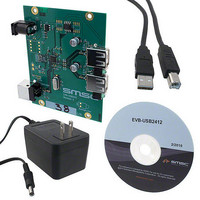
Manufacturer Part Number
EVB-USB2412
Description
EVALUATION BOARD FOR USB2412
Manufacturer
SMSC
Specifications of EVB-USB2412
Design Resources
EVB-USB2412 Schematic EVB-USB2412 BOM
Main Purpose
Interface, USB 2.0 Hub
Embedded
No
Utilized Ic / Part
USB2421
Primary Attributes
Dual Port Hub, High Speed (480Mbps)
Secondary Attributes
Single 5V Supply
Lead Free Status / RoHS Status
Lead free / RoHS Compliant
Other names
638-1106


Chapter 3 Pin Descriptions
Revision 1.0 (02-12-10)
3.1
This chapter is organized by a set of pin configurations followed by a corresponding pin list organized
by function according to their associated interface. A detailed description list of each signal (named in
the pin list) is organized by function in
to
The “N” symbol in the signal name indicates that the active, or asserted, state occurs when the signal
is at a low voltage level. When “N” is not present after the signal name, the signal is asserted when it
is at the high voltage level.
The terms assertion and negation are used exclusively. This is done to avoid confusion when working
with a mixture of “active low” and “active high” signals. The term assert, or assertion, indicates that a
signal is active, independent of whether that level is represented by a high or low voltage. The term
negate, or negation, indicates that a signal is inactive.
Pin Configuration
Table 3.3, “Buffer Type Descriptions,” on page 12
XTALIN / CLKIN
USBDM_DN[1]
USBDP_UP
XTALOUT
PLLFILT
VDD33
RBIAS
Indicates pins on the bottom of the device.
22
23
24
25
26
27
28
Figure 3.1 2-Port 28-Pin QFN
(must be connected to VSS)
(Top View QFN-28)
DATASHEET
Table 3.2, “USB2412 Pin Descriptions,” on page
USB2412
Ground Pad
SMSC
8
for a list of buffer types.
14
13
12
11
10
9
8
2-Port USB 2.0 Hi-Speed Hub Controller
VDD33
NON_REM[1]
OCS_N[2]
PRTPWR[2]
VDD33
CRFILT
OCS_N[1]
10. Please refer
SMSC USB2412
Datasheet
Related parts for EVB-USB2412
Image
Part Number
Description
Manufacturer
Datasheet
Request
R

Part Number:
Description:
BOARD EVAL FOR USB2514 48-QFN
Manufacturer:
SMSC
Datasheet:

Part Number:
Description:
Networking Modules & Development Tools LAN7500 USB 2.0 BRD 10/100/1000 GigB
Manufacturer:
SMSC
Datasheet:

Part Number:
Description:
BOARD EVAL FOR USB2514/USB2514I
Manufacturer:
SMSC
Datasheet:

Part Number:
Description:
BOARD EVAL FOR USB2512/USB2512I
Manufacturer:
SMSC
Datasheet:

Part Number:
Description:
BOARD EVAL FOR USB2513/USB2513I
Manufacturer:
SMSC
Datasheet:

Part Number:
Description:
BOARD EVALUATION FOR EMC1043
Manufacturer:
SMSC
Datasheet:
Part Number:
Description:
EVALUATION BOARD FOR USB3311C
Manufacturer:
SMSC
Datasheet:
Part Number:
Description:
EVALUATION BOARD FOR USB3317C
Manufacturer:
SMSC
Datasheet:

Part Number:
Description:
EVALUATION BOARD USB2241-AEZG
Manufacturer:
SMSC
Datasheet:

Part Number:
Description:
BOARD EVAL USB2524 SHARE/SWITCH
Manufacturer:
SMSC
Datasheet:

Part Number:
Description:
BOARD EVALUATION FOR USB2502
Manufacturer:
SMSC
Datasheet:
Part Number:
Description:
BOARD EVALUATION FOR USB2504
Manufacturer:
SMSC
Datasheet:

Part Number:
Description:
EVALUATION BOARD LAN9500-ABZJ
Manufacturer:
SMSC
Datasheet:
Part Number:
Description:
Ethernet Modules & Development Tools LAN9500 Design Kit Low-Cost USB Dongle
Manufacturer:
SMSC
Datasheet: