EVB-USB2412 SMSC, EVB-USB2412 Datasheet - Page 12
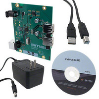
EVB-USB2412
Manufacturer Part Number
EVB-USB2412
Description
EVALUATION BOARD FOR USB2412
Manufacturer
SMSC
Specifications of EVB-USB2412
Design Resources
EVB-USB2412 Schematic EVB-USB2412 BOM
Main Purpose
Interface, USB 2.0 Hub
Embedded
No
Utilized Ic / Part
USB2421
Primary Attributes
Dual Port Hub, High Speed (480Mbps)
Secondary Attributes
Single 5V Supply
Lead Free Status / RoHS Status
Lead free / RoHS Compliant
Other names
638-1106


Revision 1.0 (02-12-10)
3.4
PIN
23
17
10
14
20
27
25
15
#
6
9
4
5
BUFFER
IPD
IPU
I/O
RESET_N
XTALOUT
SYMBOL
Buffer Type Descriptions
PLLFILT
CRFILT
VDD33
TEST
VSS
NC
Input/Output.
Input with internal weak pull-down resistor.
Input with internal weak pull-up resistor.
BUFFER
Table 3.2 USB2412 Pin Descriptions (continued)
OCLKx
TYPE
IPD
IS
POWER, GROUND, and NO CONNECTS
Table 3.3 Buffer Type Descriptions
24 MHz Crystal Output
This is the other terminal of the crystal, or a no connect pin, when an
external clock source is used to drive XTALIN/CLKIN.
TEST pin
User must treat as a no connect pin or connect to ground. No trace
or signal should be routed or attached to this pin.
RESET Input
The system can reset the chip by driving this input low. The minimum
active low pulse is 1 μs.
VDD Core Regulator Filter Capacitor
This pin must have a 1.0 μF (or greater) ±20% (ESR <0.1 Ω) capacitor
to VSS.
3.3 V Power
PLL Regulator Filter Capacitor
This pin must have a 1.0 μF (or greater) ±20% (ESR <0.1 Ω) capacitor
to VSS.
Ground Pad / ePad
The package slug is the only VSS for the device and must be tied to
ground with multiple vias.
No Connect
No signal or trace should be routed or attached to these pins.
DATASHEET
12
DESCRIPTION
DESCRIPTION
2-Port USB 2.0 Hi-Speed Hub Controller
SMSC USB2412
Datasheet
Related parts for EVB-USB2412
Image
Part Number
Description
Manufacturer
Datasheet
Request
R

Part Number:
Description:
BOARD EVAL FOR USB2514 48-QFN
Manufacturer:
SMSC
Datasheet:

Part Number:
Description:
Networking Modules & Development Tools LAN7500 USB 2.0 BRD 10/100/1000 GigB
Manufacturer:
SMSC
Datasheet:

Part Number:
Description:
BOARD EVAL FOR USB2514/USB2514I
Manufacturer:
SMSC
Datasheet:

Part Number:
Description:
BOARD EVAL FOR USB2512/USB2512I
Manufacturer:
SMSC
Datasheet:

Part Number:
Description:
BOARD EVAL FOR USB2513/USB2513I
Manufacturer:
SMSC
Datasheet:

Part Number:
Description:
BOARD EVALUATION FOR EMC1043
Manufacturer:
SMSC
Datasheet:
Part Number:
Description:
EVALUATION BOARD FOR USB3311C
Manufacturer:
SMSC
Datasheet:
Part Number:
Description:
EVALUATION BOARD FOR USB3317C
Manufacturer:
SMSC
Datasheet:

Part Number:
Description:
EVALUATION BOARD USB2241-AEZG
Manufacturer:
SMSC
Datasheet:

Part Number:
Description:
BOARD EVAL USB2524 SHARE/SWITCH
Manufacturer:
SMSC
Datasheet:

Part Number:
Description:
BOARD EVALUATION FOR USB2502
Manufacturer:
SMSC
Datasheet:
Part Number:
Description:
BOARD EVALUATION FOR USB2504
Manufacturer:
SMSC
Datasheet:

Part Number:
Description:
EVALUATION BOARD LAN9500-ABZJ
Manufacturer:
SMSC
Datasheet:
Part Number:
Description:
Ethernet Modules & Development Tools LAN9500 Design Kit Low-Cost USB Dongle
Manufacturer:
SMSC
Datasheet: