EVAL-ADF4360-8EBZ1 Analog Devices Inc, EVAL-ADF4360-8EBZ1 Datasheet - Page 21
EVAL-ADF4360-8EBZ1
Manufacturer Part Number
EVAL-ADF4360-8EBZ1
Description
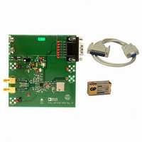
BOARD EVALUATION FOR ADF4360-8
Manufacturer
Analog Devices Inc
Datasheet
1.ADF4360-8BCPZRL7.pdf
(24 pages)
Specifications of EVAL-ADF4360-8EBZ1
Main Purpose
Timing, Frequency Synthesizer
Embedded
No
Utilized Ic / Part
ADF4360-8
Primary Attributes
Single Integer-N PLL with VCO
Secondary Attributes
120MHz, 1MHz PFD
Silicon Manufacturer
Analog Devices
Application Sub Type
Integer-N Synthesizer
Kit Application Type
Clock & Timing
Silicon Core Number
ADF4360-8
Kit Contents
Board
Frequency
400MHz
Rohs Compliant
Yes
Lead Free Status / RoHS Status
Lead free / RoHS Compliant
Other names
Q4990657


APPLICATIONS
CHOOSING THE CORRECT INDUCTANCE VALUE
The ADF4360-8 can be used at many different frequencies
simply by choosing the external inductors to give the correct
output frequency. Figure 22 shows a graph of both minimum
and maximum frequency vs. the external inductor value. The
correct inductor should cover the maximum and minimum
frequencies desired. The inductors used are 0603 CS or 0805 CS
type from Coilcraft. To reduce mutual coupling, the inductors
should be placed at right angles to one another.
The lowest center frequency of oscillation possible is approxi-
mately 65 MHz, which is achieved using 560 nH inductors. This
relationship can be expressed by
where F
tance.
The approximate value of capacitance at the midpoint of the
center band of the VCO is 9.3 pF, and the approximate value of
internal inductance due to the bond wires is 0.9 nH. The VCO
sensitivity is a measure of the frequency change vs. the tuning
voltage. It is a very important parameter for the low-pass filter.
Figure 23 shows a graph of the tuning sensitivity (in MHz/V) vs.
the inductance (nH). It can be seen that as the inductance in-
creases, the sensitivity decreases. This relationship can be de-
rived from the equation above; that is, since the inductance has
increased, the change in capacitance from the varactor has less
of an effect on the frequency.
F
Figure 22. Output Center Frequency vs. External Inductor Value
O
450
400
350
300
250
200
150
100
50
O
0
=
is the center frequency and L
0
2π
9.3
100
pF
(
0.9
1
200
nH
INDUCTANCE (nH)
+
L
EXT
300
)
EXT
400
is the external induc-
500
600
Rev. A | Page 21 of 24
FIXED FREQUENCY LO
Figure 24 shows the ADF4360-8 used as a fixed frequency LO at
200 MHz. The low-pass filter was designed using ADIsimPLL
for a channel spacing of 2 MHz and an open-loop bandwidth of
100 kHz. The maximum PFD frequency of the ADF4360-8 is
8 MHz. Since using a larger PFD frequency allows the use of a
smaller N, the in-band phase noise is reduced to as low as pos-
sible, −109 dBc/Hz. The typical rms phase noise (100 Hz to
100 kHz) of the LO in this configuration is 0.09°. The reference
frequency is from a 16MHz TCXO from Fox; thus, an R value of
2 is programmed. Taking into account the high PFD frequency
and its effect on the band select logic, the band select clock
divider is enabled. In this case, a value of 8 is chosen. A very
simple shunt inductor and dc-blocking capacitor complete the RF
output stage.
801BE-160
16MHz
FOX
1nF
Figure 23. Tuning Sensitivity (in MHz/V) vs. Inductance (nH)
10µF
12
10
8
6
4
2
0
4.7kΩ
0
1nF
1nF
51Ω
14
16
17
18
19
12
13
CPGND
100
C
REF
CLK
DATA
LE
C
R
1
V
V
N
C
SET
VCO
VCO
6
IN
Figure 24. Fixed Frequency LO
3
DV
8
21
DD
AGND DGND L1 L2 RF
200
11 22 15
ADF4360-8
AV
V
INDUCTANCE (nH)
VDD
2
DD
470Ω
CE MUXOUT
23
300
DETECT
LOCK
9
20
10
68nH
68nH
470Ω
RF
V
400
OUT
OUT
TUNE
CP
A
B
24
7
4
5
ADF4360-8
V
56nH
47pF
500
VCO
56nH
6.8kΩ
680pF
15kΩ
600
100pF
100pF
22nF
Related parts for EVAL-ADF4360-8EBZ1
Image
Part Number
Description
Manufacturer
Datasheet
Request
R

Part Number:
Description:
±1.7g Dual-Axis IMEMS Accelerometer Evaluation Board
Manufacturer:
Analog Devices Inc
Datasheet:

Part Number:
Description:
Inertial Sensor Evaluation System
Manufacturer:
Analog Devices Inc
Datasheet:
Part Number:
Description:
Manufacturer:
Analog Devices Inc
Datasheet:
Part Number:
Description:
Manufacturer:
Analog Devices Inc
Datasheet:
Part Number:
Description:
Manufacturer:
Analog Devices Inc
Datasheet:
Part Number:
Description:
Manufacturer:
Analog Devices Inc
Datasheet:
Part Number:
Description:
Manufacturer:
Analog Devices Inc
Datasheet:
Part Number:
Description:
Manufacturer:
Analog Devices Inc
Datasheet:
Part Number:
Description:
Manufacturer:
Analog Devices Inc
Datasheet:
Part Number:
Description:
Manufacturer:
Analog Devices Inc
Datasheet:
Part Number:
Description:
Manufacturer:
Analog Devices Inc
Datasheet:
Part Number:
Description:
Manufacturer:
Analog Devices Inc
Datasheet:
Part Number:
Description:
Manufacturer:
Analog Devices Inc
Datasheet: