EVAL-ADF4360-8EBZ1 Analog Devices Inc, EVAL-ADF4360-8EBZ1 Datasheet - Page 11
EVAL-ADF4360-8EBZ1
Manufacturer Part Number
EVAL-ADF4360-8EBZ1
Description
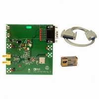
BOARD EVALUATION FOR ADF4360-8
Manufacturer
Analog Devices Inc
Datasheet
1.ADF4360-8BCPZRL7.pdf
(24 pages)
Specifications of EVAL-ADF4360-8EBZ1
Main Purpose
Timing, Frequency Synthesizer
Embedded
No
Utilized Ic / Part
ADF4360-8
Primary Attributes
Single Integer-N PLL with VCO
Secondary Attributes
120MHz, 1MHz PFD
Silicon Manufacturer
Analog Devices
Application Sub Type
Integer-N Synthesizer
Kit Application Type
Clock & Timing
Silicon Core Number
ADF4360-8
Kit Contents
Board
Frequency
400MHz
Rohs Compliant
Yes
Lead Free Status / RoHS Status
Lead free / RoHS Compliant
Other names
Q4990657


Lock Detect
MUXOUT can be programmed for one type of lock detect.
Digital lock detect is active high. When LDP in the R counter
latch is set to 0, digital lock detect is set high when the phase error
on three consecutive phase detector cycles is less than 15 ns.
With LDP set to 1, five consecutive cycles of less than 15 ns
phase error are required to set the lock detect. It stays set high
until a phase error of greater than 25 ns is detected on any
subsequent PD cycle.
INPUT SHIFT REGISTER
The ADF4360 family’s digital section includes a 24-bit input
shift register, a 14-bit R counter, and an 18-bit N counter
comprised of a 5-bit A counter and a 13-bit B counter. Data is
clocked into the 24-bit shift register on each rising edge of CLK.
The data is clocked in MSB first. Data is transferred from the
shift register to one of four latches on the rising edge of LE. The
destination latch is determined by the state of the two control
bits (C2, C1) in the shift register. The two LSBs, DB1 and DB0,
are shown in Figure 2.
The truth table for these bits is shown in Table 5. Table 6 shows
a summary of how the latches are programmed. Note that the
test modes latch is used for factory testing and should not be
programmed by the user.
Table 5. C2 and C1 Truth Table
C2
0
0
1
1
VCO
The VCO core in the ADF4360 family uses eight overlapping
bands, as shown in Figure 19, to allow a wide frequency range to
be covered without a large VCO sensitivity (K
poor phase noise and spurious performance.
Control Bits
C1
0
1
0
1
Data Latch
Control Latch
R Counter
N Counter (B)
Test Modes Latch
V
) and resultant
Rev. A | Page 11 of 24
The correct band is chosen automatically by the band select
logic at power-up or whenever the N counter latch is updated. It
is important that the correct write sequence be followed at
power-up. This sequence is
1.
2.
3.
During band select, which takes five PFD cycles, the VCO V
is disconnected from the output of the loop filter and connected
to an internal reference voltage.
The R counter output is used as the clock for the band select
logic and should not exceed 1 MHz. A programmable divider is
provided at the R counter input to allow division by 1, 2, 4, or 8,
and is controlled by the BSC1 bit and the BSC2 bit in the R
counter latch. Where the required PFD frequency exceeds
1 MHz, the divide ratio should be set to allow enough time for
correct band selection.
After band selection, normal PLL action resumes. The value of
K
Choosing the Correct Inductance Value section). The ADF4360
family contains linearization circuitry to minimize any variation
of the product of I
The operating current in the VCO core is programmable in four
steps: 2.5 mA, 5 mA, 7.5 mA, and 10 mA. This is controlled by
the PC1 bit and the PC2 bit in the control latch.
V
is determined by the value of inductors used (see the
R counter latch
Control latch
N counter latch
Figure 19. Frequency vs. V
3.5
3.0
2.5
2.0
1.5
1.0
0.5
0
80
85
CP
and K
90
FREQUENCY (MHz)
V
TUNE
.
95
, ADF4360-8, L1 and L2 = 270 nH
100
105
ADF4360-8
110
115
TUNE
Related parts for EVAL-ADF4360-8EBZ1
Image
Part Number
Description
Manufacturer
Datasheet
Request
R

Part Number:
Description:
±1.7g Dual-Axis IMEMS Accelerometer Evaluation Board
Manufacturer:
Analog Devices Inc
Datasheet:

Part Number:
Description:
Inertial Sensor Evaluation System
Manufacturer:
Analog Devices Inc
Datasheet:
Part Number:
Description:
Manufacturer:
Analog Devices Inc
Datasheet:
Part Number:
Description:
Manufacturer:
Analog Devices Inc
Datasheet:
Part Number:
Description:
Manufacturer:
Analog Devices Inc
Datasheet:
Part Number:
Description:
Manufacturer:
Analog Devices Inc
Datasheet:
Part Number:
Description:
Manufacturer:
Analog Devices Inc
Datasheet:
Part Number:
Description:
Manufacturer:
Analog Devices Inc
Datasheet:
Part Number:
Description:
Manufacturer:
Analog Devices Inc
Datasheet:
Part Number:
Description:
Manufacturer:
Analog Devices Inc
Datasheet:
Part Number:
Description:
Manufacturer:
Analog Devices Inc
Datasheet:
Part Number:
Description:
Manufacturer:
Analog Devices Inc
Datasheet:
Part Number:
Description:
Manufacturer:
Analog Devices Inc
Datasheet: