EVAL-ADF4360-8EBZ1 Analog Devices Inc, EVAL-ADF4360-8EBZ1 Datasheet - Page 20
EVAL-ADF4360-8EBZ1
Manufacturer Part Number
EVAL-ADF4360-8EBZ1
Description
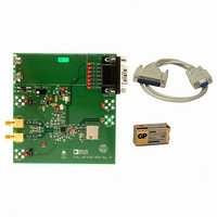
BOARD EVALUATION FOR ADF4360-8
Manufacturer
Analog Devices Inc
Datasheet
1.ADF4360-8BCPZRL7.pdf
(24 pages)
Specifications of EVAL-ADF4360-8EBZ1
Main Purpose
Timing, Frequency Synthesizer
Embedded
No
Utilized Ic / Part
ADF4360-8
Primary Attributes
Single Integer-N PLL with VCO
Secondary Attributes
120MHz, 1MHz PFD
Silicon Manufacturer
Analog Devices
Application Sub Type
Integer-N Synthesizer
Kit Application Type
Clock & Timing
Silicon Core Number
ADF4360-8
Kit Contents
Board
Frequency
400MHz
Rohs Compliant
Yes
Lead Free Status / RoHS Status
Lead free / RoHS Compliant
Other names
Q4990657


ADF4360-8
N COUNTER LATCH
Table 8 shows the input data format for programming the
N counter latch.
Reserved Bits
DB2 to DB7 are spare bits and have been designated as
reserved. They should be programmed to 0.
B Counter Latch
B13 to B1 program the B counter. The divide range is 3
(00...0011) to 8191 (11...111).
Overall Divide Range
The overall VCO feedback divide range is defined by B.
CP Gain
DB21 of the N counter latch in the ADF4360 family is the
charge pump gain bit. When it is programmed to 1, Current
Setting 2 is used. When programmed to 0, Current Setting 1 is used.
This bit can also be programmed through DB10 of the control
latch. The bit always reflects the latest value written to it, whether
this is through the control latch or the N counter latch.
Rev. A | Page 20 of 24
R COUNTER LATCH
With (C2, C1) = (0, 1), the R counter latch is programmed.
Table 9 shows the input data format for programming the
R counter latch.
R Counter
R1 to R14 set the counter divide ratio. The divide range is
1 (00...001) to 16383 (111...111).
Antibacklash Pulse Width
DB16 and DB17 set the antibacklash pulse width.
Lock Detect Precision
DB18 is the lock detect precision bit. This bit sets the number of
reference cycles with less than 15 ns phase error for entering the
locked state. With LDP at 1, five cycles are taken; with LDP at 0,
three cycles are taken.
Test Mode Bit
DB19 is the test mode bit (TMB) and should be set to 0. With
TMB = 0, the contents of the test mode latch are ignored and
normal operation occurs, as determined by the contents of the
control latch, R counter latch, and N counter latch. Note that
test modes are for factory testing only and should not be
programmed by the user.
Band Select Clock
These bits set a divider for the band select logic clock input.
The output of the R counter is, by default, the value used to
clock the band select logic; if this value is too high (>1 MHz), a
divider can be switched on to divide the R counter output to a
smaller value (see Table 9).
Reserved Bits
DB23 to DB22 are spare bits that have been designated as
reserved. They should be programmed to 0.
Related parts for EVAL-ADF4360-8EBZ1
Image
Part Number
Description
Manufacturer
Datasheet
Request
R

Part Number:
Description:
±1.7g Dual-Axis IMEMS Accelerometer Evaluation Board
Manufacturer:
Analog Devices Inc
Datasheet:

Part Number:
Description:
Inertial Sensor Evaluation System
Manufacturer:
Analog Devices Inc
Datasheet:
Part Number:
Description:
Manufacturer:
Analog Devices Inc
Datasheet:
Part Number:
Description:
Manufacturer:
Analog Devices Inc
Datasheet:
Part Number:
Description:
Manufacturer:
Analog Devices Inc
Datasheet:
Part Number:
Description:
Manufacturer:
Analog Devices Inc
Datasheet:
Part Number:
Description:
Manufacturer:
Analog Devices Inc
Datasheet:
Part Number:
Description:
Manufacturer:
Analog Devices Inc
Datasheet:
Part Number:
Description:
Manufacturer:
Analog Devices Inc
Datasheet:
Part Number:
Description:
Manufacturer:
Analog Devices Inc
Datasheet:
Part Number:
Description:
Manufacturer:
Analog Devices Inc
Datasheet:
Part Number:
Description:
Manufacturer:
Analog Devices Inc
Datasheet:
Part Number:
Description:
Manufacturer:
Analog Devices Inc
Datasheet: