EVAL-ADF4360-8EBZ1 Analog Devices Inc, EVAL-ADF4360-8EBZ1 Datasheet - Page 10
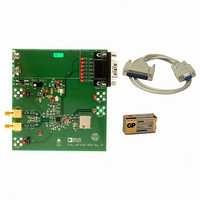
EVAL-ADF4360-8EBZ1
Manufacturer Part Number
EVAL-ADF4360-8EBZ1
Description
BOARD EVALUATION FOR ADF4360-8
Manufacturer
Analog Devices Inc
Datasheet
1.ADF4360-8BCPZRL7.pdf
(24 pages)
Specifications of EVAL-ADF4360-8EBZ1
Main Purpose
Timing, Frequency Synthesizer
Embedded
No
Utilized Ic / Part
ADF4360-8
Primary Attributes
Single Integer-N PLL with VCO
Secondary Attributes
120MHz, 1MHz PFD
Silicon Manufacturer
Analog Devices
Application Sub Type
Integer-N Synthesizer
Kit Application Type
Clock & Timing
Silicon Core Number
ADF4360-8
Kit Contents
Board
Frequency
400MHz
Rohs Compliant
Yes
Lead Free Status / RoHS Status
Lead free / RoHS Compliant
Other names
Q4990657


ADF4360-8
CIRCUIT DESCRIPTION
REFERENCE INPUT SECTION
The reference input stage is shown in Figure 16. SW1 and SW2
are normally closed switches. SW3 is normally open. When
power-down is initiated, SW3 is closed, and SW1 and SW2 are
opened. This ensures that there is no loading of the REF
on power-down.
N COUNTER
The CMOS N counter allows a wide division ratio in the PLL
feedback counter. The counters are specified to work when the
VCO output is 400 MHz or less. To avoid confusion, this is re-
ferred to as the B counter. It makes it possible to generate output
frequencies that are spaced only by the reference frequency
divided by R . The VCO frequency equation is
where:
f
B is the preset divide ratio of the binary 13-bit counter (3 to 8191).
f
R COUNTER
The 14-bit R counter allows the input reference frequency to be
divided down to produce the reference clock to the phase fre-
quency detector (PFD). Division ratios from 1 to 16,383 are
allowed.
PFD AND CHARGE PUMP
The PFD takes inputs from the R counter and N counter
( N = BP + A ) and produces an output proportional to the phase
and frequency difference between them. Figure 17 is a simpli-
fied schematic. The PFD includes a programmable delay ele-
ment that controls the width of the antibacklash pulse. This
pulse ensures that there is no dead zone in the PFD transfer
function, and minimizes phase noise and reference spurs. Two
bits in the R counter latch, ABP2 and ABP1, control the width of
the pulse (see Table 9).
VCO
REFIN
is the output frequency of the VCO.
is the external reference frequency oscillator.
f
VCO
=
REF
B
IN
×
f
NC
REFIN
POWER-DOWN
Figure 16. Reference Input Stage
SW1
CONTROL
/
NO
R
NC
SW3
SW2
100kΩ
BUFFER
TO R COUNTER
IN
pin
Rev. A | Page 10 of 24
CP OUTPUT
MUXOUT AND LOCK DETECT
The output multiplexer on the ADF4360 family allows the user
to access various internal points on the chip. The state of
MUXOUT is controlled by M3, M2, and M1 in the function
latch. The full truth table is shown in Table 7. Figure 18 shows
the MUXOUT section in block diagram form.
DIGITAL LOCK DETECT
R DIVIDER
N DIVIDER
R COUNTER OUTPUT
N COUNTER OUTPUT
R DIVIDER
N DIVIDER
HI
HI
Figure 17. PFD Simplified Schematic and Timing (In Lock)
D1
D2
CLR1
CLR2
U1
U2
Q1
Q2
PROGRAMMABLE
Figure 18. MUXOUT Circuit
ABP1
UP
DOWN
MUX
DELAY
ABP2
CONTROL
U3
CPGND
DGND
DV
V
P
DD
CHARGE
PUMP
MUXOUT
CP
Related parts for EVAL-ADF4360-8EBZ1
Image
Part Number
Description
Manufacturer
Datasheet
Request
R

Part Number:
Description:
±1.7g Dual-Axis IMEMS Accelerometer Evaluation Board
Manufacturer:
Analog Devices Inc
Datasheet:

Part Number:
Description:
Inertial Sensor Evaluation System
Manufacturer:
Analog Devices Inc
Datasheet:
Part Number:
Description:
Manufacturer:
Analog Devices Inc
Datasheet:
Part Number:
Description:
Manufacturer:
Analog Devices Inc
Datasheet:
Part Number:
Description:
Manufacturer:
Analog Devices Inc
Datasheet:
Part Number:
Description:
Manufacturer:
Analog Devices Inc
Datasheet:
Part Number:
Description:
Manufacturer:
Analog Devices Inc
Datasheet:
Part Number:
Description:
Manufacturer:
Analog Devices Inc
Datasheet:
Part Number:
Description:
Manufacturer:
Analog Devices Inc
Datasheet:
Part Number:
Description:
Manufacturer:
Analog Devices Inc
Datasheet:
Part Number:
Description:
Manufacturer:
Analog Devices Inc
Datasheet:
Part Number:
Description:
Manufacturer:
Analog Devices Inc
Datasheet:
Part Number:
Description:
Manufacturer:
Analog Devices Inc
Datasheet: