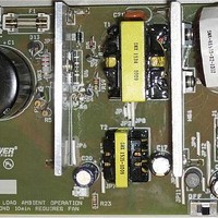
RDK-249 Power Integrations, RDK-249 Datasheet - Page 9
RDK-249
Manufacturer Part Number
RDK-249
Description
KIT REF DESIGN PFS762HG
Manufacturer
Power Integrations
Series
HiperTFS®r
Specifications of RDK-249
Main Purpose
Reference Design, PC Power Supply
Embedded
No
Utilized Ic / Part
TFS762HG
Primary Attributes
12V 25A, 5V 2.9A Outputs, 300 ~ 385 VDC Input
Output Voltage
5 V
Input / Supply Voltage (max)
385 VDC
Input / Supply Voltage (min)
300 VDC
Duty Cycle (max)
50 %
Mounting Style
Through Hole
Output Current
2.9 A
Output Power
14.5 W
Lead Free Status / RoHS Status
Lead free / RoHS Compliant
Secondary Attributes
-
Other names
596-1398


09-Nov-10
RDR-249 5 V Standby and Single 12 V Main
4.4 Output Feedback
For the Standby section, resistor R34 and R31 form a network divider. The output voltage
of the power supply is divided and fed to the input terminal of error amplifier U7. The
cathode terminal voltage of U2A is controlled by the amplifier inside U7 to maintain the
divider voltage to 2.5 V +/-2%. Change in cathode terminal voltage results in a change of
the current through optocoupler diode inside U2A, which in turn changes the current
through the transistor inside U2B. Capacitor C19 provides strong noise rejection for the
EN pin. When the current sinking from the EN pin exceeds the EN pin threshold current,
the next switching cycle is inhibited, and when the output voltage falls below the feedback
threshold, a conduction cycle is allowed to occur. By adjusting the number of enabled
cycles, output regulation is maintained. As the load reduces, the number of enabled
cycles decreases lowering the effective switching frequency and scales the switching
losses with load. This provides almost constant efficiency down to very light loads, ideal
for meeting energy efficiency requirements.
For the Main section, resistors R9 and R24 are employed to provide the DC reference for
the U5 error amplifier. In a similar manner, U5 controls the optocoupler U1 used to adjust
the operating duty cycle trough the current sink from the FB pin with the main difference
being the FB pin current controls the duty cycle of the main converter in a linear manner
versus the whole cycle on/off control of the standby converter.
4.5 Output Overvoltage Protection
The output OV protection for both Main and Standby is provided through optocoupler U4.
If the feedback loop is broken or for any other internal or external reason, the output
voltage increases over the maximum allowed limit, VR1 and/or VR2 are used to activate
the protection circuit built around U4. When the output of U4B turns on, the current flow
into the BP pin exceeds the latching shutdown threshold current of 15 mA. This will
trigger the latching shutdown feature of HiperTFS and the device stops switching,
protecting the output. The latching condition disables switching until the latch is reset with
source current into the L pin below 10 A.
Power Integrations
Tel: +1 408 414 9200 Fax: +1 408 414 9201
Page 9 of 48
www.powerint.com
Related parts for RDK-249
Image
Part Number
Description
Manufacturer
Datasheet
Request
R

Part Number:
Description:
KIT REF DESIGN TOP HX FOR TOP258
Manufacturer:
Power Integrations
Datasheet:

Part Number:
Description:
KIT REF DESIGN LINKSWITCH 2
Manufacturer:
Power Integrations
Datasheet:

Part Number:
Description:
KIT REF DESIGN 1.2W PS TN FAMILY
Manufacturer:
Power Integrations
Datasheet:

Part Number:
Description:
KIT REF DESIGN 36-72W MOTOR DRVR
Manufacturer:
Power Integrations
Datasheet:

Part Number:
Description:
KIT REF DESIGN FOR LNK457D
Manufacturer:
Power Integrations
Datasheet:

Part Number:
Description:
REFERENCE DESIGN LINKSWITCH-PH
Manufacturer:
Power Integrations
Datasheet:

Part Number:
Description:
Specifications: Manufacturer: Power Integrations ; Output Voltage: 380 VDC ; Input / Supply Voltage (Max): 264 VAC ; Input / Supply Voltage (Min): 90 VAC ; Mounting Style: Through Hole ; Output Current: 0.913 A ; Output Power: 347 W
Manufacturer:
Power Integrations, Inc.

Part Number:
Description:
Power Management Modules & Development Tools TOPSwitch-JX REF. DESIGN KIT
Manufacturer:
Power Integrations
Datasheet:
Part Number:
Description:
Power Management IC Development Tools REF DESIGN RDR-292 PFF LED STREET LIGHT
Manufacturer:
Power Integrations

Part Number:
Description:
KIT REF DESIGN FOR LNK403EG
Manufacturer:
Power Integrations
Datasheet:

Part Number:
Description:
KIT REF DESIGN FOR LNK406EG
Manufacturer:
Power Integrations
Datasheet:

Part Number:
Description:
KIT REF DESIGN DG CAPZERO
Manufacturer:
Power Integrations
Datasheet:

Part Number:
Description:
KIT REF DESIGN LINKSWITCH-CV
Manufacturer:
Power Integrations
Datasheet:
Part Number:
Description:
Specifications: Family: Eval Boards - DC/DC & AC/DC (Off-Line) SMPS ; Series: HiperLCS™ ; Main Purpose: DC/DC, Step Down ; Outputs and Type: 1, Isolated ; Power - Output: 150W ; Voltage - Output: 24V ; Current - Output: 6.25A ; Voltage - Input:
Manufacturer:
Power Integrations, Inc.
Datasheet:

Part Number:
Description:
KIT REFERENCE DESIGN W/TN376PN
Manufacturer:
Power Integrations
Datasheet: