RDK-249 Power Integrations, RDK-249 Datasheet - Page 7
RDK-249
Manufacturer Part Number
RDK-249
Description
KIT REF DESIGN PFS762HG
Manufacturer
Power Integrations
Series
HiperTFS®r
Specifications of RDK-249
Main Purpose
Reference Design, PC Power Supply
Embedded
No
Utilized Ic / Part
TFS762HG
Primary Attributes
12V 25A, 5V 2.9A Outputs, 300 ~ 385 VDC Input
Output Voltage
5 V
Input / Supply Voltage (max)
385 VDC
Input / Supply Voltage (min)
300 VDC
Duty Cycle (max)
50 %
Mounting Style
Through Hole
Output Current
2.9 A
Output Power
14.5 W
Lead Free Status / RoHS Status
Lead free / RoHS Compliant
Secondary Attributes
-
Other names
596-1398


09-Nov-10
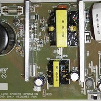
RDR-249 5 V Standby and Single 12 V Main
4 Circuit Description
The HiperTFS TFS762HG cost effectively incorporates a low-side 725 V Main MOSFET,
a high-side 530 V Main MOSFET and a 725 V Standby MOSFET, main and standby
controllers, a high-side driver along with thermal shutdown and other fault protection and
other control circuitry in a single package. The device is well suited for high power
applications with both main and standby converter (such as PC power supplies). The
standby operates over a wide input voltage range. The main converter is intended to
accept boosted input voltage from a power-factor correction stage and normally operates
over a range from 385 VDC to 300 VDC
4.1 Power Input and Filter
This circuit is designed for PC power supplies with a Main output power up to 300 W.
Diode D13 provides protection against catastrophic failure in case of reverse input
voltage connection which would cause fuse F1 to open. Capacitor C1 is the bulk energy
storage element providing energy for at least 20 ms at full load from 385 VDC initial input
voltage.
4.2 Primary Side
Components C2, R1, R6 and VR3 form a turn-off clamping circuit that limits the drain
voltage of U6 for both the standby drain and the drain of the low-side Main Drain of the
forward converter. Zener VR3 provides a defined clamp voltage and maintains a
maximum voltage (150 V) on clamp capacitor C2. Most of the leakage and magnetizing
energy is returned back to converter due to the slow recovery aspect of the general
recovery diodes D3 and D4. Shared reset/leakage spike clamp between Main and
Standby reduces component count. The Standby is connected via diode D3 and resistor
R5 and the Main section is connected through D8 and D4 together with R7 and R8.
During the reset time, the Main section is connected to a substantially higher reset
voltage than V
, hence the Main operating duty cycle of the Main converter can operate
IN
above 50% which lowers RMS switch currents without penalizing holdup time.
The BYPASS (BP) pin along with C12 provides a decoupled operating voltage for the
HiperTFS controller. At start-up the bypass capacitor is charged from an internal device
current source. When the BP pin voltage reaches 5.8 V the standby converter will begin
switching and both the +5 V standby output and primary-side bias voltage will begin to
rise. The output of the bias/auxiliary supply winding is rectified by diode D12 and filtered
by capacitor C20. Output of the bias winding is used to supply power via resistor R16 to
the HiperTFS BP pin during standby only operation. Additional current is provided by Q1
and D10 by the primary bias supply when remote-on switch SW1 activates U3A and U3B
and commands Q1 into an ON state. In a complete PC power supply application, this
voltage is used to supply bias to the PFC controller through J4 connector. The value of
R16 is selected to maintain the minimum 700 A required into BP pin to inhibit the
internal HiperTFS high voltage current source and thus reduce no-load consumption.
Capacitor C12 connected to the BP pin of U6 provides decoupling for the internally
Power Integrations
Tel: +1 408 414 9200 Fax: +1 408 414 9201
Page 7 of 48
www.powerint.com
Related parts for RDK-249
Image
Part Number
Description
Manufacturer
Datasheet
Request
R

Part Number:
Description:
KIT REF DESIGN TOP HX FOR TOP258
Manufacturer:
Power Integrations
Datasheet:

Part Number:
Description:
KIT REF DESIGN LINKSWITCH 2
Manufacturer:
Power Integrations
Datasheet:

Part Number:
Description:
KIT REF DESIGN 1.2W PS TN FAMILY
Manufacturer:
Power Integrations
Datasheet:

Part Number:
Description:
KIT REF DESIGN 36-72W MOTOR DRVR
Manufacturer:
Power Integrations
Datasheet:

Part Number:
Description:
KIT REF DESIGN FOR LNK457D
Manufacturer:
Power Integrations
Datasheet:

Part Number:
Description:
REFERENCE DESIGN LINKSWITCH-PH
Manufacturer:
Power Integrations
Datasheet:

Part Number:
Description:
Specifications: Manufacturer: Power Integrations ; Output Voltage: 380 VDC ; Input / Supply Voltage (Max): 264 VAC ; Input / Supply Voltage (Min): 90 VAC ; Mounting Style: Through Hole ; Output Current: 0.913 A ; Output Power: 347 W
Manufacturer:
Power Integrations, Inc.

Part Number:
Description:
Power Management Modules & Development Tools TOPSwitch-JX REF. DESIGN KIT
Manufacturer:
Power Integrations
Datasheet:
Part Number:
Description:
Power Management IC Development Tools REF DESIGN RDR-292 PFF LED STREET LIGHT
Manufacturer:
Power Integrations

Part Number:
Description:
KIT REF DESIGN FOR LNK403EG
Manufacturer:
Power Integrations
Datasheet:

Part Number:
Description:
KIT REF DESIGN FOR LNK406EG
Manufacturer:
Power Integrations
Datasheet:

Part Number:
Description:
KIT REF DESIGN DG CAPZERO
Manufacturer:
Power Integrations
Datasheet:

Part Number:
Description:
KIT REF DESIGN LINKSWITCH-CV
Manufacturer:
Power Integrations
Datasheet:
Part Number:
Description:
Specifications: Family: Eval Boards - DC/DC & AC/DC (Off-Line) SMPS ; Series: HiperLCS™ ; Main Purpose: DC/DC, Step Down ; Outputs and Type: 1, Isolated ; Power - Output: 150W ; Voltage - Output: 24V ; Current - Output: 6.25A ; Voltage - Input:
Manufacturer:
Power Integrations, Inc.
Datasheet:

Part Number:
Description:
KIT REFERENCE DESIGN W/TN376PN
Manufacturer:
Power Integrations
Datasheet: