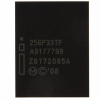
RC28F256P33TFA NUMONYX, RC28F256P33TFA Datasheet - Page 67

RC28F256P33TFA
Manufacturer Part Number
RC28F256P33TFA
Description
IC FLASH 256MBIT 95NS 64EZBGA
Manufacturer
NUMONYX
Series
Axcell™r
Specifications of RC28F256P33TFA
Format - Memory
FLASH
Memory Type
FLASH
Memory Size
256M (16Mx16)
Speed
95ns
Interface
Parallel
Voltage - Supply
2.3 V ~ 3.6 V
Operating Temperature
-40°C ~ 85°C
Package / Case
64-EZBGA
Cell Type
NOR
Density
256Mb
Interface Type
Parallel/Serial
Boot Type
Top
Address Bus
25b
Operating Supply Voltage (typ)
2.5/3/3.3V
Operating Temp Range
-40C to 85C
Package Type
EZBGA
Sync/async
Async/Sync
Operating Temperature Classification
Industrial
Operating Supply Voltage (min)
2.3V
Operating Supply Voltage (max)
3.6V
Word Size
16b
Number Of Words
32M
Supply Current
50mA
Mounting
Surface Mount
Pin Count
64
Lead Free Status / RoHS Status
Contains lead / RoHS non-compliant
Other names
902063
902063
RC28F256P33TF 902063
902063
RC28F256P33TF 902063
Available stocks
Company
Part Number
Manufacturer
Quantity
Price
Company:
Part Number:
RC28F256P33TFA
Manufacturer:
Micron Technology Inc
Quantity:
10 000
P33-65nm
Figure 30: Burst Read Information
Table 36: Partition and Erase Block Region Information
Datasheet
67
P = 10Ah
Offset
(P+1D)h
(P+1E)h
(P+1F)h
(P+20)h
(P+21)h
(P+22)h
Bottom
(P+23)h
P = 10Ah
Offset
(1)
Length
(P+23)h
(1)
Top
1
1
1
1
1
1
Page Mode Read capability
bits 0–7 = “n” such that 2
Number of synchronous mode read configuration fields that follow . 00h
indicates no burst capability.
Synchronous mode read capability configuration 1
continuous synchronous reads w hen the device is configured for its maximum
w ord w idth. A value of 07h indicates that the device is capable of continuous
linear bursts that w ill output data until the internal burst counter reaches the end
of the device’s burstable address space. This field’s 3-bit value can be w ritten
directly to the Read Configuration Register bits 0–2 if the device is configured
for its maximum w ord w idth. See offset 28h for w ord w idth to determine the
burst data output w idth.
Synchronous mode read capability configuration 2
Synchronous mode read capability configuration 3
Synchronous mode read capability configuration 4
Number of device hardw are-partition regions w ithin the device.
read-page bytes. See offset 28h for device w ord w idth to
determine page-mode data output w idth. 00h indicates no
read page buffer.
Bits 3–7 = Reserved
Bits 0–2 “n” such that 2n+1 HEX value represents the maximum number of
x = 0: a single hardw are partition device (no fields follow ).
x specifies the number of device partition regions containing
one or more contiguous erase block regions.
(Optional flash features and commands)
(Optional flash features and commands)
n
HEX value represents the number of
Description
Description
Order Number:320003-09
Add.
12A:
127:
128:
129:
12B:
12C:
Len
1
See table below
Code
Hex
12D:
--05
--04
--01
--02
--03
--07
Bot
Address
Mar 2010
32 byte
Value
12D:
Cont
Top
16
4
4
8


