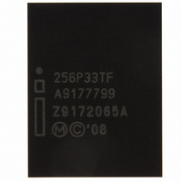
RC28F256P33TFA NUMONYX, RC28F256P33TFA Datasheet - Page 41

RC28F256P33TFA
Manufacturer Part Number
RC28F256P33TFA
Description
IC FLASH 256MBIT 95NS 64EZBGA
Manufacturer
NUMONYX
Series
Axcell™r
Specifications of RC28F256P33TFA
Format - Memory
FLASH
Memory Type
FLASH
Memory Size
256M (16Mx16)
Speed
95ns
Interface
Parallel
Voltage - Supply
2.3 V ~ 3.6 V
Operating Temperature
-40°C ~ 85°C
Package / Case
64-EZBGA
Cell Type
NOR
Density
256Mb
Interface Type
Parallel/Serial
Boot Type
Top
Address Bus
25b
Operating Supply Voltage (typ)
2.5/3/3.3V
Operating Temp Range
-40C to 85C
Package Type
EZBGA
Sync/async
Async/Sync
Operating Temperature Classification
Industrial
Operating Supply Voltage (min)
2.3V
Operating Supply Voltage (max)
3.6V
Word Size
16b
Number Of Words
32M
Supply Current
50mA
Mounting
Surface Mount
Pin Count
64
Lead Free Status / RoHS Status
Contains lead / RoHS non-compliant
Other names
902063
902063
RC28F256P33TF 902063
902063
RC28F256P33TF 902063
Available stocks
Company
Part Number
Manufacturer
Quantity
Price
Company:
Part Number:
RC28F256P33TFA
Manufacturer:
Micron Technology Inc
Quantity:
10 000
P33-65nm
Figure 12: OTP Register Map
11.2.1
Datasheet
41
The OTP Registers contain OTP bits; when programmed, PR bits cannot be erased. Each
OTP Register can be accessed multiple times to program individual bits, as long as the
register remains unlocked.
Each OTP Register has an associated Lock Register bit. When a Lock Register bit is
programmed, the associated OTP Register can only be read; it can no longer be
programmed. Additionally, because the Lock Register bits themselves are OTP, when
programmed, Lock Register bits cannot be erased. Therefore, when a OTP Register is
locked, it cannot be unlocked.
.
Reading the OTP Registers
The OTP Registers can be read from any address. To read the OTP Register, first issue
the Read Device Identifier command at any address to place the device in the Read
Device Identifier state (see
Next, perform a read operation using the address offset corresponding to the register
to be read.
offsets of the OTP Registers and Lock Registers. PR data is read 16 bits at a time.
Table 8, “Device Identifier Information” on page 22
0x109
0x102
0x8A
0x91
0x89
0x88
0x85
0x84
0x81
0x80
15 14 13 12 11 10 9
15 14 13 12 11 10 9
128-bit Protection Register 16
128-bit Protection Register 1
128-Bit Protection Register 0
(Factory-Programmed)
(User-Programmable)
(User-Programmable)
(User-Programmable)
Lock Register 1
64-bit Segment
64-bit Segment
Section 6.2, “Device Command Bus Cycles” on page
Lock Register 0
8
8
7
7
6
6
5
5
4
4
3
3
2
2
1
1
0
0
shows the address
Order Number:320003-09
Mar 2010
18).


