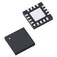
PIC16F721-I/ML Microchip Technology, PIC16F721-I/ML Datasheet - Page 23

PIC16F721-I/ML
Manufacturer Part Number
PIC16F721-I/ML
Description
MCU PIC 4K FLASH 20-QFN
Manufacturer
Microchip Technology
Series
PIC® XLP™ 16Fr
Datasheets
1.PIC16F722-ISS.pdf
(8 pages)
2.PIC16LF720-ISS.pdf
(244 pages)
3.PIC16F720-ISO.pdf
(36 pages)
4.PIC16F720-ISO.pdf
(8 pages)
5.PIC16F721-IML.pdf
(6 pages)
Specifications of PIC16F721-I/ML
Core Size
8-Bit
Program Memory Size
7KB (4K x 14)
Peripherals
Brown-out Detect/Reset, POR, PWM, WDT
Core Processor
PIC
Speed
16MHz
Connectivity
I²C, SPI, UART/USART
Number Of I /o
17
Program Memory Type
FLASH
Ram Size
256 x 8
Voltage - Supply (vcc/vdd)
1.8 V ~ 5.5 V
Data Converters
A/D 12x8b
Oscillator Type
Internal
Operating Temperature
-40°C ~ 85°C
Package / Case
20-VFQFN Exposed Pad
Controller Family/series
PIC16F
No. Of I/o's
18
Ram Memory Size
256Byte
Cpu Speed
16MHz
No. Of Timers
3
Lead Free Status / RoHS Status
Lead free / RoHS Compliant
Eeprom Size
-
Lead Free Status / RoHS Status
Lead free / RoHS Compliant
7.0
In the hex file there are two bytes per program word
stored in the Intel
LSB first, MSB second. Because there are two bytes
per word, the addresses in the hex file are 2x the
address
Configuration Word 1 is stored at 2007h on the
PIC16F/LF720 and PIC16F/LF721. In the hex file this
will be at location 400Eh-400Fh).
7.1
To allow portability of code, it is strongly recommended
that the programmer is able to read the Configuration
Words and user ID locations from the hex file. If the
Configuration Words information was not present in the
hex file, a simple warning message may be issued.
Similarly, while saving a hex file, Configuration Words
and user ID information should be included.
7.2
If a device ID is present in the hex file at 400Ch-400Dh
(2006h on the part), the programmer should verify the
device ID (excluding the revision) against the value
read from the part. On a mismatch condition, the
programmer should generate a warning message.
EXAMPLE 7-1:
2011 Microchip Technology Inc.
PIC16F720
Note 1: Sum of Memory addresses = (Total number of program memory address locations) x (3FFFh) = F800h,
HEX FILE USAGE
Configuration Word
Device ID and Revision
2: Configuration Word 1 and 2 = all bits are ‘1’; thus, code-protect is disabled.
3: Configuration Word 1 and 2 Mask = all bits are set to ‘1’, except for unimplemented bits that are ‘0’.
in
truncated to 16 bits.
program
®
Sum of Memory addresses 0000h-07FFh
Configuration Word 1
Configuration Word 1 mask
Configuration Word 2
Configuration Word 2 mask
Checksum
INH8M hex format. Data is stored
CHECKSUM COMPUTED WITH CODE PROTECTION DISABLED (PIC16F720),
BLANK DEVICE
memory.
(Example:
(2)
(2)
= F800h + (3FFFh and 337Bh) + (3FFFh and 0013h)
= F800h + 337Bh + 0013h
= 2B8Eh
Advance Information
(3)
(3)
The
(1)
7.3
The checksum is calculated by two different methods,
dependent on the setting of the CP Configuration bit.
TABLE 7-1:
7.3.1
With the code protection disabled, the checksum is
computed by reading the contents of the PIC16F/
LF720 and PIC16F/LF721 program memory locations
and adding up the program memory data, starting at
address 0000h, up to the maximum user addressable
location, 0FFFh for the PIC16F/LF720 and 07FFh for
the PIC16F/LF721. Any Carry bit exceeding 16 bits are
neglected. Additionally, the relevant bits of the Config-
uration Words are added to the checksum. All unused
Configuration bits are masked to ‘0’. See
Configuration Word Mask Values.
Example 7-1
a blank device and for a device with 00AAh at the first
and last program memory locations.
PIC16F720
PIC16LF720
PIC16F721
PIC16LF721
Device
PIC16(L)F720/721
Checksum Computation
F800h
3FFFh
337Bh
3FFFh
0013h
CODE PROTECTION DISABLED
through
CONFIGURATION WORD
MASK VALUES
Config. Word 1
Example 7-4
337Bh
337Bh
337Bh
337Bh
Mask
shown below are for
DS41409B-page 23
Config. Word 2
Table 7-1
0013h
0003h
0013h
0003h
Mask
for


