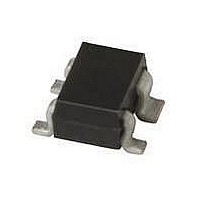
BFG410W,135 NXP Semiconductors, BFG410W,135 Datasheet - Page 4

BFG410W,135
Manufacturer Part Number
BFG410W,135
Description
TRANS RF NPN 22GHZ 4.5V SOT343
Manufacturer
NXP Semiconductors
Datasheet
1.BFG410W115.pdf
(13 pages)
Specifications of BFG410W,135
Package / Case
SC-82A, SOT-343
Transistor Type
NPN
Voltage - Collector Emitter Breakdown (max)
4.5V
Frequency - Transition
22GHz
Noise Figure (db Typ @ F)
0.9dB ~ 1.2dB @ 900MHz ~ 2GHz
Gain
21dB
Power - Max
54mW
Dc Current Gain (hfe) (min) @ Ic, Vce
50 @ 10mA, 2V
Current - Collector (ic) (max)
12mA
Mounting Type
Surface Mount
Dc Collector/base Gain Hfe Min
50
Dc Current Gain Hfe Max
120
Mounting Style
SMD/SMT
Configuration
Single
Transistor Polarity
NPN
Collector- Emitter Voltage Vceo Max
4.5 V
Emitter- Base Voltage Vebo
1 V
Continuous Collector Current
10 mA
Power Dissipation
54 mW
Lead Free Status / RoHS Status
Lead free / RoHS Compliant
NXP Semiconductors
CHARACTERISTICS
T
Notes
1. G
2. Z
1998 Mar 11
V
V
V
I
h
C
C
C
f
G
F
P
ITO
SYMBOL
j
CBO
T
S
FE
= 25 C unless otherwise specified.
(BR)CBO
(BR)CEO
(BR)EBO
L1
NPN 22 GHz wideband transistor
c
e
re
max
21
S
max
2
is optimized for noise; Z
is the maximum power gain, if K > 1. If K < 1 then G
collector-base breakdown voltage
collector-emitter breakdown
voltage
emitter-base breakdown voltage
collector-base leakage current
DC current gain
collector capacitance
emitter capacitance
feedback capacitance
transition frequency
maximum power gain; note 1
insertion power gain
noise figure
output power at 1 dB gain
compression
third order intercept point
PARAMETER
L
is optimized for gain.
I
I
I
I
I
I
I
I
I
I
I
see Fig.4
T
T
T
I
f = 900 MHz;
I
I
Z
I
Z
C
C
E
E
C
E
C
C
C
C
C
C
C
C
C
amb
amb
amb
S
S
S
= 2.5 A; I
= 0; V
= i
= 2.5 A; I
= 1 mA; I
= 10 mA; V
= i
= 0; V
= 10 mA; V
= 10 mA; V
= 10 mA; V
= 1 mA; V
= 1 mA; V
= 10 mA; V
= 10 mA; V
=
= Z
= Z
e
c
= 25 C; see Fig.5
= 25 C; see Figs 7 and 8
= 25 C; see Fig.8
= 0; V
= 0; V
opt
S opt
S opt
CB
CB
; see Fig.13
4
CONDITIONS
; Z
; Z
= 4.5 V
= 2 V; f = 1 MHz;
B
max
CB
EB
CE
CE
C
E
L
L
= 0
CE
CE
CE
CE
CE
CE
= 0
= 0
= Z
= Z
S
= 2 V; f = 1 MHz
= 0.5 V; f = 1 MHz
= 2 V;
= 2 V; f = 2 GHz;
= MSG; see Figs 6, 7 and 8.
=
= 2 V; see Fig.3
= 2 V; f = 2 GHz;
= 2 V; f = 2 GHz;
= 2 V; f = 2 GHz;
= 2 V; f = 2 GHz;
= 2 V; f = 2 GHz;
L opt
L opt
opt
; note 2
; note 2
; see Fig.13
10
4.5
1
50
MIN.
80
220
400
45
22
21
18
0.9
1.2
5
15
TYP.
Product specification
BFG410W
15
120
MAX.
V
V
V
nA
fF
fF
fF
GHz
dB
dB
dB
dB
dBm
dBm
UNIT


