IXXH50N60C3D1 IXYS, IXXH50N60C3D1 Datasheet - Page 2
IXXH50N60C3D1
Manufacturer Part Number
IXXH50N60C3D1
Description
IGBT 600V 100A 600W TO247AD
Manufacturer
IXYS
Series
XPT™, GenX3™r
Datasheet
1.IXXH50N60C3D1.pdf
(7 pages)
Specifications of IXXH50N60C3D1
Igbt Type
PT
Voltage - Collector Emitter Breakdown (max)
600V
Vce(on) (max) @ Vge, Ic
2.3V @ 15V, 36A
Current - Collector (ic) (max)
100A
Power - Max
600W
Input Type
Standard
Mounting Type
Through Hole
Package / Case
TO-247-3 (TO-247AD)
Collector- Emitter Voltage Vceo Max
600 V
Collector-emitter Saturation Voltage
2.3 V
Maximum Gate Emitter Voltage
20 V
Continuous Collector Current At 25 C
100 A
Gate-emitter Leakage Current
100 nA
Power Dissipation
600 W
Maximum Operating Temperature
+ 175 C
Minimum Operating Temperature
- 55 C
Mounting Style
Through Hole
Channel Type
N
Configuration
Single
Collector-emitter Voltage
600V
Collector Current (dc) (max)
100A
Gate To Emitter Voltage (max)
±20V
Package Type
TO-247AD
Pin Count
3
Mounting
Through Hole
Operating Temperature (min)
-55C
Operating Temperature (max)
175C
Operating Temperature Classification
Military
Vces, (v)
600
Ic25, Tc = 25°c, Igbt, (a)
100
Ic90, Tc = 90°c, Igbt, (a)
-
Ic110, Tc = 110°c, Igbt, (a)
50
Vce(sat), Typ, Tj = 25°c, Igbt (v)
2.3
Tfi, Typ, Tj = 25°c, Igbt, (ns)
42
Eoff, Typ, Tj = 125°c, Igbt (mj)
-
Eoff, Typ, Tj = 150°c, Igbt (mj)
0.48
Rthjc, Max, Igbt (c/w)
0.25
If, Tc = 90°c, Diode (a)
-
If, Tc = 110°c, Diode (a)
30
Rthjc, Max, Diode (k/w)
0.90
Package Style
TO-247
Lead Free Status / RoHS Status
Lead free / RoHS Compliant


Symbol Test Conditions
(T
g
C
C
C
Q
Q
Q
t
t
E
t
t
E
t
t
E
t
t
E
R
R
Reverse Diode (FRED)
Symbol Test Conditions
(T
V
I
t
R
Notes:
IXYS Reserves the Right to Change Limits, Test Conditions, and Dimensions.
IXYS MOSFETs and IGBTs are covered
by one or more of the following U.S. patents: 4,850,072
RM
d(on)
ri
d(off)
fi
d(on)
ri
d(off)
fi
rr
fs
F
ie
oes
res
on
of
on
off
thJC
thCS
thJC
g
ge
gc
J
J
The product presented herein is under development. The Technical Specifications offered are derived
from a subjective evaluation of the design, based upon prior knowledge and experience, and constitute a
"considered reflection" of the anticipated result. IXYS reserves the right to change limits, test
conditions, and dimensions without notice.
s
f
= 25°C Unless Otherwise Specified)
= 25°C Unless Otherwise Specified)
1. Pulse test, t ≤ 300μs, duty cycle, d ≤ 2%.
2. Switching times & energy losses may increase for higher V
I
I
V
I
F
F
F
R
= 24A, V
= 30A, V
= 100V
= 1A, V
V
I
Inductive load, T
I
V
Note 2
Inductive load, T
I
V
Note 2
I
C
C
C
C
CE
CE
CE
=
= 36A, V
= 36A, V
=
= 25V, V
= 360V, R
= 360V, R
36A
36A
GE
GE
ADVANCE TECHNICAL INFORMATION
GE
= 0V, -di
= 0V, Note 1
, V
= 0V, -di
, V
GE
GE
GE
CE
GE
= 15V
= 15V
= 15V, V
G
G
= 10V, Note 1
= 0V, f = 1MHz
= 5
= 5
F
4,835,592
4,881,106
F
/dt = 100A/μs, V
/dt = 100A/μs,
J
J
Ω
Ω
= 25°C
= 150°C
CE
4,931,844
5,017,508
5,034,796
= 0.5
•
R
V
= 30V
CES
5,049,961
5,063,307
5,187,117
T
T
T
J
J
J
= 150°C
= 100°C
= 100°C
Min.
5,237,481
5,381,025
5,486,715
11
Characteristic Values
Characteristic Values
Min.
6,162,665
6,259,123 B1
6,306,728 B1
2320
0.72
0.33
1.46
0.48
0.21
Typ.
138
18
42
64
18
25
24
40
62
42
25
44
80
90
CE
Typ.
1.6
100
(clamp), T
25
Max.
0.55
0.25 °C/W
100
6,404,065 B1
6,534,343
6,583,505
0.9 °C/W
Max.
2.7
4
J
°C/W
or R
mJ
mJ
mJ
mJ
nC
nC
nC
pF
pF
pF
ns
ns
ns
ns
ns
ns
ns
ns
ns
ns
S
V
V
A
G
.
6,683,344
6,710,405 B2 6,759,692
6,710,463
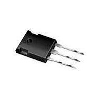
IXXH50N60C3D1
TO-247 (IXXH) Outline
Terminals: 1 - Gate
6,727,585
6,771,478 B2 7,071,537
Dim.
A
A
A
b
b
b
C
D
E
e
L
L1
∅P
Q
R
S
1
2
1
2
20.80
15.75
19.81
1.65
2.87
5.20
3.55
5.89
4.32
6.15 BSC
Min.
Millimeter
4.7
2.2
2.2
1.0
3 - Emitted
1
.4
7,005,734 B2
7,063,975 B2
2
21.46
16.26
20.32
Max.
2.54
2.13
3.12
5.72
4.50
3.65
6.40
5.49
3
5.3
2.6
1.4
.8
e
2 - Collector
0.205 0.225
0.232 0.252
∅ P
.185
.087
.059
.040
.065
.113
.016
.819
.610
.780
.140
.170
Min.
242 BSC
Inches
7,157,338B2
Max.
.209
.102
.098
.055
.084
.123
.031
.845
.640
.800
.177
.144
.216
Related parts for IXXH50N60C3D1
Image
Part Number
Description
Manufacturer
Datasheet
Request
R


Part Number:
Description:
HiPerFET Power MOSFETs
Manufacturer:
IXYS Corporation
Datasheet:
Part Number:
Description:
J-K-Type Flip-Flop
Manufacturer:
IXYS Corporation
Datasheet:
Part Number:
Description:
HiPerRF Power MOSFETs
Manufacturer:
IXYS Corporation
Datasheet:
Part Number:
Description:
Rectifier Module for Three Phase Power Factor Correction
Manufacturer:
IXYS Corporation
Datasheet:
Part Number:
Description:
Thyristor Modules Thyristor/Diode Modules
Manufacturer:
IXYS Corporation
Datasheet:
Part Number:
Description:
Thyristor Modules Thyristor/Diode Modules
Manufacturer:
IXYS Corporation
Datasheet:
Part Number:
Description:
Thyristor Modules Thyristor/Diode Modules
Manufacturer:
IXYS Corporation
Datasheet:
Part Number:
Description:
Thyristor Modules Thyristor/Diode Modules
Manufacturer:
IXYS Corporation
Datasheet:
Part Number:
Description:
Thyristor Modules /Diode Modules
Manufacturer:
IXYS Corporation
Datasheet:
Part Number:
Description:
Thyristor Modules /Diode Modules
Manufacturer:
IXYS Corporation
Datasheet:
Part Number:
Description:
Thyristor Modules Thyristor/Diode Modules
Manufacturer:
IXYS Corporation
Datasheet: