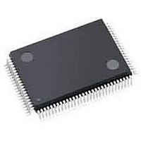
A54SX08A-TQG100 Actel, A54SX08A-TQG100 Datasheet - Page 62

A54SX08A-TQG100
Manufacturer Part Number
A54SX08A-TQG100
Description
FPGA - Field Programmable Gate Array 12K System Gates
Manufacturer
Actel
Datasheet
1.A54SX08A-TQG100.pdf
(108 pages)
Specifications of A54SX08A-TQG100
Processor Series
A54SX08
Core
IP Core
Number Of Macrocells
512
Maximum Operating Frequency
350 MHz
Number Of Programmable I/os
130
Delay Time
4 ns to 8.4 ns
Supply Voltage (max)
5.25 V
Maximum Operating Temperature
+ 70 C
Minimum Operating Temperature
0 C
Development Tools By Supplier
Silicon-Explorer II, Silicon-Sculptor 3, SI-EX-TCA
Mounting Style
SMD/SMT
Supply Voltage (min)
2.25 V
Number Of Gates
8000
Package / Case
TQFP-100
Lead Free Status / RoHS Status
Lead free / RoHS Compliant
Available stocks
Company
Part Number
Manufacturer
Quantity
Price
Company:
Part Number:
A54SX08A-TQG100
Manufacturer:
Microsemi SoC
Quantity:
10 000
Part Number:
A54SX08A-TQG100
Manufacturer:
MICROSEMI/美高森美
Quantity:
20 000
Company:
Part Number:
A54SX08A-TQG100A
Manufacturer:
Microsemi SoC
Quantity:
10 000
Company:
Part Number:
A54SX08A-TQG100I
Manufacturer:
Microsemi SoC
Quantity:
10 000
Table 2-35 • A54SX72A Timing Characteristics
2 -4 2
Parameter
C-Cell Propagation Delays
t
Predicted Routing Delays
t
t
t
t
t
t
t
t
R-Cell Timing
t
t
t
t
t
t
t
t
t
Input Module Propagation Delays
t
t
t
t
t
t
Notes:
1. All –3 speed grades have been discontinued.
2. For dual-module macros, use t
3. Routing delays are for typical designs across worst-case operating conditions. These parameters should be used for estimating device
PD
DC
FC
RD1
RD2
RD3
RD4
RD8
RD12
RCO
CLR
PRESET
SUD
HD
WASYN
RECASYN
HASYN
MPW
INYH
INYL
INYH
INYL
INYH
INYL
SX-A Family FPGAs
performance. Post-route timing analysis or simulation is required to determine actual performance.
(Worst-Case Commercial Conditions, V
Internal Array Module
FO = 1 Routing Delay, Direct
Connect
FO = 1 Routing Delay, Fast Connect
FO = 1 Routing Delay
FO = 2 Routing Delay
FO = 3 Routing Delay
FO = 4 Routing Delay
FO = 8 Routing Delay
FO = 12 Routing Delay
Sequential Clock-to-Q
Asynchronous Clear-to-Q
Asynchronous Preset-to-Q
Flip-Flop Data Input Set-Up
Flip-Flop Data Input Hold
Asynchronous Pulse Width
Asynchronous Recovery Time
Asynchronous Hold Time
Clock Minimum Pulse Width
Input Data Pad to Y High 2.5 V
LVCMOS
Input Data Pad to Y Low 2.5 V
LVCMOS
Input Data Pad to Y High 3.3 V PCI
Input Data Pad to Y Low 3.3 V PCI
Input Data Pad to Y High 3.3 V
LVTTL
Input Data Pad to Y Low 3.3 V LVTTL
Description
3
2
PD
+ t
RD1
+ t
PDn
, t
RCO
Min. Max. Min. Max. Min. Max. Min. Max. Min. Max.
–3 Speed
0.7
0.0
0.3
0.3
1.3
1.5
CCA
+ t
RD1
= 2.25 V
1.0
0.1
0.3
0.3
0.4
0.5
0.7
1.2
1.7
0.7
0.6
0.7
0.6
0.8
0.6
0.7
0.7
1.0
+ t
1
v5.3
PDn
,
–2 Speed
0.8
0.0
1.5
0.4
0.3
1.7
V
, or t
CCI
= 3.0 V, T
PD1
1.1
0.1
0.3
0.5
0.9
2.2
0.8
0.7
1.0
0.7
0.8
0.7
0.3
0.7
1.5
0.7
0.8
1.2
+ t
RD1
0.9
0.0
1.7
0.4
0.3
2.0
–1 Speed
J
+ t
= 70°C)
SUD
1.3
0.1
0.3
0.4
0.6
0.8
1.7
2.5
0.9
0.7
0.8
0.8
1.1
0.7
0.9
0.8
1.3
, whichever is appropriate.
1
Std. Speed
1.0
0.0
2.0
0.5
0.4
2.3
1.5
0.1
0.4
0.5
0.7
0.9
1.1
2.1
1.1
0.9
1.0
0.9
1.3
0.9
1.0
1.0
1.5
3
1.4
0.0
2.8
0.7
0.6
3.2
–F Speed
2.0
0.1
0.6
0.7
1.3
1.5
2.9
4.2
1.5
1.2
1.4
1.3
1.7
1.2
1.4
1.4
2.1
1
Units
ns
ns
ns
ns
ns
ns
ns
ns
ns
ns
ns
ns
ns
ns
ns
ns
ns
ns
ns
ns
ns
ns
ns
ns


