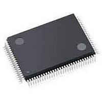
A54SX08A-TQG100 Actel, A54SX08A-TQG100 Datasheet - Page 39

A54SX08A-TQG100
Manufacturer Part Number
A54SX08A-TQG100
Description
FPGA - Field Programmable Gate Array 12K System Gates
Manufacturer
Actel
Datasheet
1.A54SX08A-TQG100.pdf
(108 pages)
Specifications of A54SX08A-TQG100
Processor Series
A54SX08
Core
IP Core
Number Of Macrocells
512
Maximum Operating Frequency
350 MHz
Number Of Programmable I/os
130
Delay Time
4 ns to 8.4 ns
Supply Voltage (max)
5.25 V
Maximum Operating Temperature
+ 70 C
Minimum Operating Temperature
0 C
Development Tools By Supplier
Silicon-Explorer II, Silicon-Sculptor 3, SI-EX-TCA
Mounting Style
SMD/SMT
Supply Voltage (min)
2.25 V
Number Of Gates
8000
Package / Case
TQFP-100
Lead Free Status / RoHS Status
Lead free / RoHS Compliant
Available stocks
Company
Part Number
Manufacturer
Quantity
Price
Company:
Part Number:
A54SX08A-TQG100
Manufacturer:
Microsemi SoC
Quantity:
10 000
Part Number:
A54SX08A-TQG100
Manufacturer:
MICROSEMI/美高森美
Quantity:
20 000
Company:
Part Number:
A54SX08A-TQG100A
Manufacturer:
Microsemi SoC
Quantity:
10 000
Company:
Part Number:
A54SX08A-TQG100I
Manufacturer:
Microsemi SoC
Quantity:
10 000
Table 2-14 • A54SX08A Timing Characteristics (Continued)
Parameter
t
t
t
t
Input Module Predicted Routing Delays
t
t
t
t
t
t
Notes:
1. For dual-module macros, use t
2. Routing delays are for typical designs across worst-case operating conditions. These parameters should be used for estimating device
INYH
INYL
INYH
INYL
IRD1
IRD2
IRD3
IRD4
IRD8
IRD12
performance. Post-route timing analysis or simulation is required to determine actual performance.
(Worst-Case Commercial Conditions, V
Input Data Pad to Y High 5 V PCI
Input Data Pad to Y Low 5 V PCI
Input Data Pad to Y High 5 V TTL
Input Data Pad to Y Low 5 V TTL
FO = 1 Routing Delay
FO = 2 Routing Delay
FO = 3 Routing Delay
FO = 4 Routing Delay
FO = 8 Routing Delay
FO = 12 Routing Delay
Description
PD
+ t
RD1
+ t
PDn
2
, t
RCO
CCA
+ t
RD1
= 2.25 V
+ t
Min. Max. Min. Max. Min.
v5.3
PDn
–2 Speed
,
V
, or t
CCI
0.5
0.8
0.5
0.8
0.3
0.5
0.6
0.8
1.4
= 3.0 V, T
2
PD1
+ t
RD1
–1 Speed
J
+ t
= 70°C)
SUD
0.6
0.9
0.6
0.9
0.3
0.5
0.7
0.9
1.5
2.2
, whichever is appropriate.
Std. Speed
Max. Min. Max.
0.7
1.1
0.7
1.1
0.4
0.6
0.8
1.8
2.6
1
–F Speed
SX-A Family FPGAs
0.9
1.5
0.9
1.5
0.6
0.8
1.1
1.4
2.5
3.6
Units
ns
ns
ns
ns
ns
ns
ns
ns
ns
ns
2-19


