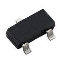
TP5335K1-G Supertex, TP5335K1-G Datasheet - Page 2

TP5335K1-G
Manufacturer Part Number
TP5335K1-G
Description
MOSFET Small Signal 350V 25Ohm
Manufacturer
Supertex
Datasheet
1.TP5335K1-G.pdf
(3 pages)
Specifications of TP5335K1-G
Minimum Operating Temperature
- 55 C
Configuration
Single
Transistor Polarity
P-Channel
Resistance Drain-source Rds (on)
30 Ohm @ 10 V
Drain-source Breakdown Voltage
350 V
Gate-source Breakdown Voltage
+/- 20 V
Continuous Drain Current
0.085 A
Power Dissipation
360 mW
Maximum Operating Temperature
+ 150 C
Mounting Style
SMD/SMT
Package / Case
SOT-23
Lead Free Status / RoHS Status
Lead free / RoHS Compliant
Switching Waveforms and Test Circuit
Thermal Characteristics
Notes:
Electrical Characteristics
Notes:
ΔR
ΔV
R
V
BV
†
Sym
t
1.
2.
I
C
C
t
TO-236AB (SOT-23)
C
d(OFF)
I
I
G
V
GS(TH)
D(ON)
DS(ON)
d(ON)
GSS
DSS
GS(TH)
DS(ON)
t
OSS
RSS
t
t
ISS
SD
rr
DSS
FS
r
f
I
D
All D.C. parameters 100% tested at 25
All A.C. parameters sample tested.
(continuous) is limited by max rated T
Package
OUTPUT
INPUT
Parameter
Drain-to-source breakdown voltage
Gate threshold voltage
Change in V
Gate body leakage current
Zero gate voltage drain current
On-state drain current
Static drain-to-source on-state
resistance
Change in R
Forward transconductance
Input capacitance
Common source output capacitance
Reverse transfer capacitance
Turn-on delay time
Rise time
Turn-off delay time
Fall time
Diode forward voltage drop
Reverse recovery time
-10V
V
0V
0V
DD
10%
GS(TH)
DS(ON)
t
d(ON)
(continuous)
10%
with temperature
t
with temperature
(ON)
(mA)
-85
●
t
I
r
D
1235 Bordeaux Drive, Sunnyvale, CA 94089
90%
J
O
.
C unless otherwise stated. (Pulse test: 300µs pulse, 2% duty cycle.)
(T
†
A
= 25
90%
t
d(OFF)
O
(pulsed)
C unless otherwise specified)
t
90%
(OFF)
-400
(mA)
I
D
t
F
10%
Power Dissipation
-350
-200
-400
Min
-1.0
125
-
-
-
-
-
-
-
-
-
-
-
-
-
-
-
-
-
2
@T
0.36
A
(W)
= 25
Typ
800
-
-
-
-
-
-
-
-
-
-
-
-
-
-
-
-
-
-
-
-
-
GENERATOR
O
C
PULSE
●
Tel: 408-222-8888
-100
Max
-2.4
-1.0
-5.0
-1.8
INPUT
110
R
4.5
-10
1.7
75
30
60
22
20
15
25
25
GEN
-
-
-
-
-
(
O
200
C/W)
θ
jc
mV/
mmho
Units
%/
mA
mA
nA
µA
nA
pF
ns
ns
Ω
V
V
V
O
O
C
C
●
(
O
350
www.supertex.com
C/W)
θ
Conditions
V
V
V
V
V
V
V
V
V
V
V
V
V
V
V
V
f = 1MHz
V
I
R
V
V
D
ja
GS
DS
DS
GS
DS
DS
GS
GS
GS
GS
GS
GS
GS
DS
GS
DS
DD
GEN
GS
GS
= -150mA,
= 0V, I
= V
= V
= ±20V, V
= Max rating, V
= 0.8 Max Rating,
= 0V, T
= 0V, V
= -4.5V, V
= -10V, V
= -4.5V, I
= -10V, I
= -10V, I
= -25V, I
= 0V,
= -25V,
= -25V,
= 0V, I
= 0V, I
= 25Ω,
GS
GS
V
R
DD
, I
, I
L
(mA)
I
-85
D
SD
SD
DR
A
D
D
DS
= -100µA
Output
D.U.T.
= 125
D
D
D
= -1.0mA
= -1.0mA
†
= -200mA
= -200mA
D
DS
= -330V
DS
= -200mA
DS
= -200mA
= -200mA
= -150mA
= -25V
= 0V
TP5335
= -25V
O
C
GS
-400
(mA)
I
DRM
= 0V


