TWR-S08MM128-KIT Freescale Semiconductor, TWR-S08MM128-KIT Datasheet - Page 14
TWR-S08MM128-KIT
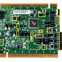
Manufacturer Part Number
TWR-S08MM128-KIT
Description
MCU, MPU & DSP Development Tools For 9S08MM128 USB CAN
Manufacturer
Freescale Semiconductor
Datasheet
1.MC9S08MM128CMB.pdf
(52 pages)
Specifications of TWR-S08MM128-KIT
Processor To Be Evaluated
9S08MM128
Data Bus Width
8 bit
Interface Type
USB, CAN
Silicon Manufacturer
Freescale
Core Architecture
Coldfire, HCS08
Core Sub-architecture
Coldfire V1, HCS08
Silicon Core Number
MCF51, MC9S08
Silicon Family Name
Flexis - MCF51MM, Flexis - S08MM
Rohs Compliant
Yes
Lead Free Status / RoHS Status
Lead free / RoHS Compliant


Electrical Characteristics
2.2
Absolute maximum ratings are stress ratings only, and functional operation at the maxima is not guaranteed. Stress beyond the
limits specified in the following table may affect device reliability or cause permanent damage to the device. For functional
operating conditions, refer to the remaining tables in this section.
This device contains circuitry protecting against damage due to high static voltage or electrical fields; however, it is advised
that normal precautions be taken to avoid application of any voltages higher than maximum-rated voltages to this
high-impedance circuit. Reliability of operation is enhanced if unused inputs are tied to an appropriate logic voltage level (for
instance, either V
14
Freescale reserves the right to change the detail specifications as may be required to permit improvements in the design of its products.
Absolute Maximum Ratings
1
2
3
current-limiting resistor, calculate resistance values for positive (V
voltages, then use the larger of the two resistance values.
All functional non-supply pins are internally clamped to V
Power supply must maintain regulation within operating V
maximum current conditions. If positive injection current (V
current may flow out of V
external V
risk when the MCU is not consuming power. Examples are: if no system clock is present, or if the clock
rate is very low (which would reduce overall power consumption).
#
1
2
3
4
5
Input must be current limited to the value specified. To determine the value of the required
SS
Supply voltage
Maximum current into V
Digital input voltage
Instantaneous maximum current
Storage temperature range
or V
Single pin limit (applies to all port pins)
DD
DD
load will shunt current greater than maximum injection current. This will be the greatest
).
DD
Rating
Table 5. Absolute Maximum Ratings
and could result in external power supply going out of regulation. Ensure
DD
1, 2, 3
DD
SS
In
range during instantaneous and operating
Symbol
and V
> V
V
T
I
V
DD
I
DD
stg
D
In
DD
DD
DD
) is greater than I
) and negative (V
.
–0.3 to V
–0.3 to +3.8
–55 to 150
Value
25
120
DD
DD
+ 0.3
SS
, the injection
Freescale Semiconductor
) clamp
Unit
mA
mA
C
V
V
Related parts for TWR-S08MM128-KIT
Image
Part Number
Description
Manufacturer
Datasheet
Request
R

Part Number:
Description:
TOWER SYSTEM BOARD MC9S08MM128
Manufacturer:
Freescale Semiconductor
Datasheet:

Part Number:
Description:
Development Boards & Kits - S08 / S12 S08PT60 Tower Kit
Manufacturer:
Freescale Semiconductor
Datasheet:
Part Number:
Description:
Development Boards & Kits - S08 / S12 S08PT60Tower MCU mod
Manufacturer:
Freescale Semiconductor
Datasheet:
Part Number:
Description:
TOWER UNIVERSAL RS08/S08
Manufacturer:
Freescale Semiconductor
Datasheet:

Part Number:
Description:
Manufacturer:
Freescale Semiconductor, Inc
Datasheet:
Part Number:
Description:
Manufacturer:
Freescale Semiconductor, Inc
Datasheet:
Part Number:
Description:
Manufacturer:
Freescale Semiconductor, Inc
Datasheet:
Part Number:
Description:
Manufacturer:
Freescale Semiconductor, Inc
Datasheet:
Part Number:
Description:
Manufacturer:
Freescale Semiconductor, Inc
Datasheet:
Part Number:
Description:
Manufacturer:
Freescale Semiconductor, Inc
Datasheet:
Part Number:
Description:
Manufacturer:
Freescale Semiconductor, Inc
Datasheet:
Part Number:
Description:
Manufacturer:
Freescale Semiconductor, Inc
Datasheet:
Part Number:
Description:
Manufacturer:
Freescale Semiconductor, Inc
Datasheet:
Part Number:
Description:
Manufacturer:
Freescale Semiconductor, Inc
Datasheet:
Part Number:
Description:
Manufacturer:
Freescale Semiconductor, Inc
Datasheet: