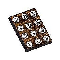
FSA2269UCX Fairchild Semiconductor, FSA2269UCX Datasheet

FSA2269UCX
Specifications of FSA2269UCX
Available stocks
Related parts for FSA2269UCX
FSA2269UCX Summary of contents
Page 1
... LCD Monitor, TV, and Set-Top Box Ordering Information Part Number Top Mark FSA2269L10X HL FSA2269UMX HP FSA2269TSL10X HU FSA2269TSUMX HT FSA2269UCX N9 Analog Symbols 1B0 1B1 2B0 2B1 Figure 1. FSA2269 © 2007 Fairchild Semiconductor Corporation FSA2269 / FSA2269TS • Rev. 1.1.3 Low-Voltage Dual-SPDT (0.4Ω) Description The FSA2269 is a high-performance, dual Single-Pole ) for +3 ...
Page 2
... Pin # UMLP Micropak Truth Table Control Input, Sn LOW Logic Level HIGH Logic Level © 2007 Fairchild Semiconductor Corporation FSA2269 / FSA2269TS • Rev. 1.1.3 1B1 1 10 1B0 Figure 4. 10-Pin MicroPak™ (Top Through View) WLCSP Name B1 1B1 D3 2B0 B3 2B1 B2,C2 GND C3 2A ...
Page 3
... Fairchild Semiconductor Corporation FSA2269 / FSA2269TS • Rev. 1.1.3 Parameter 1B0, 1B1, 2B0, 2B1, 1A, 2A Pins (1) S1, S2 Pulsed at 1ms Duration, <10% Duty Cycle Soldering, 10 Seconds I/O to GND I/O to GND FSA2269UCX Power to GND All Other Pins Parameter 3 Min. Max. Unit -0.5 5.5 ...
Page 4
... Port Only 1A, 2A) (FSA2269TS) Switch (3,6) Resistance On Resistance ∆R Matching Between ON (4) Channels © 2007 Fairchild Semiconductor Corporation FSA2269 / FSA2269TS • Rev. 1.1.3 Conditions V (V) CC 3.60 to 4.50 3.00 to 3.60 2.70 to 3.00 2.30 to 2.70 1.65 to 1.95 3.60 to 4.50 2.70 to 3.60 2.30 to 2.70 1 ...
Page 5
... R measured at identical max ON min 5. Flatness is defined as the difference between the maximum and minimum value of on resistance (R specified range of conditions. 6. Guaranteed by characterization, not production tested. © 2007 Fairchild Semiconductor Corporation FSA2269 / FSA2269TS • Rev. 1.1.3 (Continued) Conditions V (V) CC 4.50 3.00 I =100mA, nB0 or ...
Page 6
... Break-Before- nB1=1.5V, t Make Time BBM R =50Ω, L FSA2269 C =35pF L nB0 or Break-Before- nB1=1.5V, t Make Time BBM R =50Ω, L FSA2269UCX C =35pF L nB0 or Break-Before- nB1=1.5V, t Make Time BBM R =50Ω, L FSA2269TS C =35pF L © 2007 Fairchild Semiconductor Corporation FSA2269 / FSA2269TS • Rev. 1.1.3 T =+25ºC ...
Page 7
... Distortion BIAS Capacitance Symbol Parameter C Control Pin Input Capacitance Port Off Capacitance OFF C A Port On Capacitance ON © 2007 Fairchild Semiconductor Corporation FSA2269 / FSA2269TS • Rev. 1.1.3 (Continued (V) CC Min. 1.65 to 4.50 =0Ω S 1.65 to 4.50 1.65 to 4.50 1.65 to 4.50 1.65 to 4.50 =2V PP ...
Page 8
... Test Diagrams GND Figure 7. On Resistance Select V Sel Figure 9. On Leakage © 2007 Fairchild Semiconductor Corporation FSA2269 / FSA2269TS • Rev. 1.1 Select GND = Sel A(ON) A(ON GND = 2.5ns t RISE V CC 90% 90% Input - V Sel 10% GND V OH 90% Output - V OUT OFF Figure 11. Turn-On / Turn-Off Waveforms ...
Page 9
... GND R and C L environment (see AC/DC tables). C includes test fixture and stray capacitance GND R and R S environment (see AC/DC tables). © 2007 Fairchild Semiconductor Corporation FSA2269 / FSA2269TS • Rev. 1.1 OUT GND are functions of the application L L Figure 12. Break-Before-Make Interval Timing ...
Page 10
... GND nB n Capacitance Meter f = 1MHz nB Figure 17. Channel Off Capacitance GND R S environment (see AC Tables for specific values). © 2007 Fairchild Semiconductor Corporation FSA2269 / FSA2269TS • Rev. 1.1.3 NC GND R T GND GND are functions of the application T CROSSTALK = 20 Log (V Figure 15. Adjacent Channel Crosstalk B Input – ...
Page 11
... Package drawings are provided as a service to customers considering Fairchild components. Drawings may change in any manner without notice. Please note the revision and/or date on the drawing and contact a Fairchild Semiconductor representative to verify or obtain the most recent revision. Package specifications do not expand the terms of Fairchild’s worldwide terms and conditions, specifically the warranty therein, which covers Fairchild products. Always visit Fairchild Semiconductor’ ...
Page 12
... Package drawings are provided as a service to customers considering Fairchild components. Drawings may change in any manner without notice. Please note the revision and/or date on the drawing and contact a Fairchild Semiconductor representative to verify or obtain the most recent revision. Package specifications do not expand the terms of Fairchild’s worldwide terms and conditions, specifically the warranty therein, which covers Fairchild products. Always visit Fairchild Semiconductor’ ...
Page 13
... BOTTOM VIEW Product Specific Dimensions Product FSA2269UCX 1.560mm Figure 22. 12-Ball, Wafer Level Chip-Scale Package (WLCSP) Package drawings are provided as a service to customers considering Fairchild components. Drawings may change in any manner without notice. Please note the revision and/or date on the drawing and contact a Fairchild Semiconductor representative to verify or obtain the most recent revision. Package specifications do not expand the terms of Fairchild’ ...
Page 14
... Fairchild Semiconductor Corporation FSA2269 / FSA2269TS • Rev. 1.1.3 14 www.fairchildsemi.com ...


