S9S08DN32F1MLC Freescale Semiconductor, S9S08DN32F1MLC Datasheet - Page 272
S9S08DN32F1MLC
Manufacturer Part Number
S9S08DN32F1MLC
Description
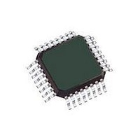
IC MCU 8BIT 32KB FLASH 32LQFP
Manufacturer
Freescale Semiconductor
Series
HCS08r
Specifications of S9S08DN32F1MLC
Core Processor
HCS08
Core Size
8-Bit
Speed
40MHz
Connectivity
I²C, LIN, SCI, SPI
Peripherals
LVD, POR, PWM, WDT
Number Of I /o
25
Program Memory Size
32KB (32K x 8)
Program Memory Type
FLASH
Eeprom Size
1K x 8
Ram Size
1.5K x 8
Voltage - Supply (vcc/vdd)
2.7 V ~ 5.5 V
Data Converters
A/D 10x12b
Oscillator Type
Internal
Operating Temperature
-40°C ~ 125°C
Package / Case
32-LQFP
Processor Series
S08D
Core
HCS08
Data Bus Width
8 bit
Data Ram Size
1 KB
Interface Type
I2C, SCI, SPI
Maximum Clock Frequency
40 MHz
Number Of Programmable I/os
26
Operating Supply Voltage
3 V to 5 V
Maximum Operating Temperature
+ 125 C
Mounting Style
SMD/SMT
3rd Party Development Tools
EWS08
Development Tools By Supplier
DEMO9S08DZ60
Minimum Operating Temperature
- 40 C
On-chip Adc
12 bit, 10 Channel
Lead Free Status / RoHS Status
Lead free / RoHS Compliant
Available stocks
Company
Part Number
Manufacturer
Quantity
Price
Company:

Part Number:
S9S08DN32F1MLC
Manufacturer:
Freescale Semiconductor
Quantity:
10 000
Part Number:
S9S08DN32F1MLC
Manufacturer:
FREESCALE
Quantity:
20 000


Chapter 15 Timer/PWM Module (S08TPMV3)
15.3.5
These read/write registers contain the captured TPM counter value of the input capture function or the
output compare value for the output compare or PWM functions. The channel registers are cleared by
reset.
272
ELSnB
ELSnA
MSnA
Field
3–2
4
Mode select A for TPM channel n. When CPWMS=0 and MSnB=0, MSnA configures TPM channel n for
input-capture mode or output compare mode. Refer to
controls.
Note: If the associated port pin is not stable for at least two bus clock cycles before changing to input capture
Edge/level select bits. Depending upon the operating mode for the timer channel as set by CPWMS:MSnB:MSnA
and shown in
the level that will be driven in response to an output compare match, or select the polarity of the PWM output.
Setting ELSnB:ELSnA to 0:0 configures the related timer pin as a general purpose I/O pin not related to any timer
functions. This function is typically used to temporarily disable an input capture channel or to make the timer pin
available as a general purpose I/O pin when the associated timer channel is set up as a software timer that does
not require the use of a pin.
TPM Channel Value Registers (TPMxCnVH:TPMxCnVL)
CPWMS
X
0
1
mode, it is possible to get an unexpected indication of an edge trigger.
Table
MSnB:MSnA
Table 15-5. TPMxCnSC Field Descriptions (continued)
15-6, these bits select the polarity of the input edge that triggers an input capture event, select
XX
XX
1X
00
01
Table 15-6. Mode, Edge, and Level Selection
MC9S08DN60 Series Data Sheet, Rev 3
ELSnB:ELSnA
X1
X1
00
01
10
11
01
10
11
10
10
Description
Output compare
Center-aligned
Input capture
Edge-aligned
Table 15-6
Pin not used for TPM - revert to general
purpose I/O or other peripheral control
Mode
PWM
PWM
for a summary of channel mode and setup
Capture on falling edge
Capture on rising edge
Set output on compare
High-true pulses (clear
High-true pulses (clear
output on compare-up)
output on compare-up)
Low-true pulses (set
Low-true pulses (set
Capture on rising or
output on compare)
output on compare)
Toggle output on
Clear output on
Configuration
falling edge
compare
compare
only
only
Freescale Semiconductor
Related parts for S9S08DN32F1MLC
Image
Part Number
Description
Manufacturer
Datasheet
Request
R

Part Number:
Description:
Manufacturer:
Freescale Semiconductor, Inc
Datasheet:
Part Number:
Description:
Manufacturer:
Freescale Semiconductor, Inc
Datasheet:
Part Number:
Description:
Manufacturer:
Freescale Semiconductor, Inc
Datasheet:
Part Number:
Description:
Manufacturer:
Freescale Semiconductor, Inc
Datasheet:
Part Number:
Description:
Manufacturer:
Freescale Semiconductor, Inc
Datasheet:
Part Number:
Description:
Manufacturer:
Freescale Semiconductor, Inc
Datasheet:
Part Number:
Description:
Manufacturer:
Freescale Semiconductor, Inc
Datasheet:
Part Number:
Description:
Manufacturer:
Freescale Semiconductor, Inc
Datasheet:
Part Number:
Description:
Manufacturer:
Freescale Semiconductor, Inc
Datasheet:
Part Number:
Description:
Manufacturer:
Freescale Semiconductor, Inc
Datasheet:
Part Number:
Description:
Manufacturer:
Freescale Semiconductor, Inc
Datasheet:
Part Number:
Description:
Manufacturer:
Freescale Semiconductor, Inc
Datasheet:
Part Number:
Description:
Manufacturer:
Freescale Semiconductor, Inc
Datasheet:
Part Number:
Description:
Manufacturer:
Freescale Semiconductor, Inc
Datasheet:
Part Number:
Description:
Manufacturer:
Freescale Semiconductor, Inc
Datasheet: