S9S08DN32F1MLC Freescale Semiconductor, S9S08DN32F1MLC Datasheet - Page 106
S9S08DN32F1MLC
Manufacturer Part Number
S9S08DN32F1MLC
Description
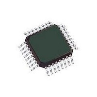
IC MCU 8BIT 32KB FLASH 32LQFP
Manufacturer
Freescale Semiconductor
Series
HCS08r
Specifications of S9S08DN32F1MLC
Core Processor
HCS08
Core Size
8-Bit
Speed
40MHz
Connectivity
I²C, LIN, SCI, SPI
Peripherals
LVD, POR, PWM, WDT
Number Of I /o
25
Program Memory Size
32KB (32K x 8)
Program Memory Type
FLASH
Eeprom Size
1K x 8
Ram Size
1.5K x 8
Voltage - Supply (vcc/vdd)
2.7 V ~ 5.5 V
Data Converters
A/D 10x12b
Oscillator Type
Internal
Operating Temperature
-40°C ~ 125°C
Package / Case
32-LQFP
Processor Series
S08D
Core
HCS08
Data Bus Width
8 bit
Data Ram Size
1 KB
Interface Type
I2C, SCI, SPI
Maximum Clock Frequency
40 MHz
Number Of Programmable I/os
26
Operating Supply Voltage
3 V to 5 V
Maximum Operating Temperature
+ 125 C
Mounting Style
SMD/SMT
3rd Party Development Tools
EWS08
Development Tools By Supplier
DEMO9S08DZ60
Minimum Operating Temperature
- 40 C
On-chip Adc
12 bit, 10 Channel
Lead Free Status / RoHS Status
Lead free / RoHS Compliant
Available stocks
Company
Part Number
Manufacturer
Quantity
Price
Company:

Part Number:
S9S08DN32F1MLC
Manufacturer:
Freescale Semiconductor
Quantity:
10 000
Part Number:
S9S08DN32F1MLC
Manufacturer:
FREESCALE
Quantity:
20 000


Chapter 6 Parallel Input/Output Control
6.5.7.3
6.5.7.4
Note: Slew rate reset default values may differ between engineering samples and final production parts. Always initialize slew
106
PTGPE[5:0]
PTGSE[5:0]
Reset:
Reset:
Field
Field
5:0
5:0
rate control to the desired value to ensure correct operation.
W
W
R
R
Internal Pull Enable for Port G Bits — Each of these control bits determines if the internal pull-up device is
enabled for the associated PTG pin. For port G pins that are configured as outputs, these bits have no effect and
the internal pull devices are disabled.
0 Internal pull-up device disabled for port G bit n.
1 Internal pull-up device enabled for port G bit n.
Output Slew Rate Enable for Port G Bits — Each of these control bits determines if the output slew rate control
is enabled for the associated PTG pin. For port G pins that are configured as inputs, these bits have no effect.
0 Output slew rate control disabled for port G bit n.
1 Output slew rate control enabled for port G bit n.
Port G Pull Enable Register (PTGPE)
0
0
Port G Slew Rate Enable Register (PTGSE)
0
0
7
7
Pull-down devices only apply when using pin interrupt functions, when
corresponding edge select and pin select functions are configured.
= Unimplemented or Reserved
= Unimplemented or Reserved
Figure 6-44. Internal Pull Enable for Port G Register (PTGPE)
Figure 6-45. Slew Rate Enable for Port G Register (PTGSE)
0
0
0
0
6
6
Table 6-42. PTGPE Register Field Descriptions
Table 6-43. PTGSE Register Field Descriptions
PTGPE5
PTGSE5
MC9S08DN60 Series Data Sheet, Rev 3
0
0
5
5
PTGPE4
PTGSE4
NOTE
0
0
4
4
Description
Description
PTGPE3
PTGSE3
3
0
3
0
PTGPE2
PTGSE2
0
0
2
2
PTGPE1
PTGSE1
Freescale Semiconductor
0
0
1
1
PTGPE0
PTGSE0
0
0
0
0
Related parts for S9S08DN32F1MLC
Image
Part Number
Description
Manufacturer
Datasheet
Request
R

Part Number:
Description:
Manufacturer:
Freescale Semiconductor, Inc
Datasheet:
Part Number:
Description:
Manufacturer:
Freescale Semiconductor, Inc
Datasheet:
Part Number:
Description:
Manufacturer:
Freescale Semiconductor, Inc
Datasheet:
Part Number:
Description:
Manufacturer:
Freescale Semiconductor, Inc
Datasheet:
Part Number:
Description:
Manufacturer:
Freescale Semiconductor, Inc
Datasheet:
Part Number:
Description:
Manufacturer:
Freescale Semiconductor, Inc
Datasheet:
Part Number:
Description:
Manufacturer:
Freescale Semiconductor, Inc
Datasheet:
Part Number:
Description:
Manufacturer:
Freescale Semiconductor, Inc
Datasheet:
Part Number:
Description:
Manufacturer:
Freescale Semiconductor, Inc
Datasheet:
Part Number:
Description:
Manufacturer:
Freescale Semiconductor, Inc
Datasheet:
Part Number:
Description:
Manufacturer:
Freescale Semiconductor, Inc
Datasheet:
Part Number:
Description:
Manufacturer:
Freescale Semiconductor, Inc
Datasheet:
Part Number:
Description:
Manufacturer:
Freescale Semiconductor, Inc
Datasheet:
Part Number:
Description:
Manufacturer:
Freescale Semiconductor, Inc
Datasheet:
Part Number:
Description:
Manufacturer:
Freescale Semiconductor, Inc
Datasheet: