ATMEGA48PA-MNR Atmel, ATMEGA48PA-MNR Datasheet - Page 164
ATMEGA48PA-MNR
Manufacturer Part Number
ATMEGA48PA-MNR
Description
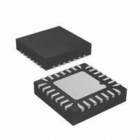
MCU AVR 4KB FLASH 20MHZ 28QFN
Manufacturer
Atmel
Series
AVR® ATmegar
Datasheet
1.ATMEGA48PA-AN.pdf
(448 pages)
Specifications of ATMEGA48PA-MNR
Core Processor
AVR
Core Size
8-Bit
Speed
20MHz
Connectivity
I²C, SPI, UART/USART
Peripherals
Brown-out Detect/Reset, POR, PWM, WDT
Number Of I /o
23
Program Memory Size
4KB (2K x 16)
Program Memory Type
FLASH
Eeprom Size
256 x 8
Ram Size
512 x 8
Voltage - Supply (vcc/vdd)
1.8 V ~ 5.5 V
Data Converters
A/D 8x10b
Oscillator Type
Internal
Operating Temperature
-40°C ~ 85°C
Package / Case
*
Core
AVR8
Data Bus Width
8 bit
Data Ram Size
512 B
Interface Type
SPI, UART, I2C
Maximum Clock Frequency
20 MHz
Number Of Programmable I/os
23
Operating Supply Voltage
1.8 V to 5.5 V
Maximum Operating Temperature
+ 105 C
Mounting Style
SMD/SMT
Operating Temperature Range
- 40 C to + 85 C
Processor To Be Evaluated
ATMEGA48A
Lead Free Status / RoHS Status
Lead free / RoHS Compliant


17.11.8
8161D–AVR–10/09
ASSR – Asynchronous Status Register
• Bit 7 – RES: Reserved bit
This bit is reserved and will always read as zero.
• Bit 6 – EXCLK: Enable External Clock Input
When EXCLK is written to one, and asynchronous clock is selected, the external clock input buf-
fer is enabled and an external clock can be input on Timer Oscillator 1 (TOSC1) pin instead of a
32 kHz crystal. Writing to EXCLK should be done before asynchronous operation is selected.
Note that the crystal Oscillator will only run when this bit is zero.
• Bit 5 – AS2: Asynchronous Timer/Counter2
When AS2 is written to zero, Timer/Counter2 is clocked from the I/O clock, clk
written to one, Timer/Counter2 is clocked from a crystal Oscillator connected to the Timer Oscil-
lator 1 (TOSC1) pin. When the value of AS2 is changed, the contents of TCNT2, OCR2A,
OCR2B, TCCR2A and TCCR2B might be corrupted.
• Bit 4 – TCN2UB: Timer/Counter2 Update Busy
When Timer/Counter2 operates asynchronously and TCNT2 is written, this bit becomes set.
When TCNT2 has been updated from the temporary storage register, this bit is cleared by hard-
ware. A logical zero in this bit indicates that TCNT2 is ready to be updated with a new value.
• Bit 3 – OCR2AUB: Output Compare Register2 Update Busy
When Timer/Counter2 operates asynchronously and OCR2A is written, this bit becomes set.
When OCR2A has been updated from the temporary storage register, this bit is cleared by hard-
ware. A logical zero in this bit indicates that OCR2A is ready to be updated with a new value.
• Bit 2 – OCR2BUB: Output Compare Register2 Update Busy
When Timer/Counter2 operates asynchronously and OCR2B is written, this bit becomes set.
When OCR2B has been updated from the temporary storage register, this bit is cleared by hard-
ware. A logical zero in this bit indicates that OCR2B is ready to be updated with a new value.
• Bit 1 – TCR2AUB: Timer/Counter Control Register2 Update Busy
When Timer/Counter2 operates asynchronously and TCCR2A is written, this bit becomes set.
When TCCR2A has been updated from the temporary storage register, this bit is cleared by
hardware. A logical zero in this bit indicates that TCCR2A is ready to be updated with a new
value.
• Bit 0 – TCR2BUB: Timer/Counter Control Register2 Update Busy
When Timer/Counter2 operates asynchronously and TCCR2B is written, this bit becomes set.
When TCCR2B has been updated from the temporary storage register, this bit is cleared by
hardware. A logical zero in this bit indicates that TCCR2B is ready to be updated with a new
value.
If a write is performed to any of the five Timer/Counter2 Registers while its update busy flag is
set, the updated value might get corrupted and cause an unintentional interrupt to occur.
Bit
(0xB6)
Read/Write
Initial Value
R
7
–
0
EXCLK
R/W
6
0
AS2
R/W
5
0
ATmega48PA/88PA/168PA/328P
TCN2UB
4
R
0
OCR2AUB
R
3
0
OCR2BUB
R
2
0
TCR2AUB
R
1
0
TCR2BUB
I/O
. When AS2 is
R
0
0
ASSR
164
Related parts for ATMEGA48PA-MNR
Image
Part Number
Description
Manufacturer
Datasheet
Request
R

Part Number:
Description:
Manufacturer:
Atmel Corporation
Datasheet:

Part Number:
Description:
MCU AVR 4K ISP FLASH 20MHZ 32QFN
Manufacturer:
Atmel
Datasheet:

Part Number:
Description:
MCU AVR 4K ISP FLSH 20MHZ 32TQFP
Manufacturer:
Atmel
Datasheet:

Part Number:
Description:
MCU AVR 4K ISP FLASH 20MHZ 28DIP
Manufacturer:
Atmel
Datasheet:
Part Number:
Description:
MCU AVR 4K FLASH 20MHZ 32TQFP
Manufacturer:
Atmel
Datasheet:

Part Number:
Description:
MCU AVR 4K FLASH 20MHZ 32QFN
Manufacturer:
Atmel
Datasheet:

Part Number:
Description:
MCU AVR 4K FLASH 20MHZ 28-QFN
Manufacturer:
Atmel
Datasheet:
Part Number:
Description:
MCU AVR 4K FLASH 20MHZ 28QFN
Manufacturer:
Atmel
Datasheet:
Part Number:
Description:
IC AVR MCU 4K 5V 20MHZ 32-TQFP
Manufacturer:
Atmel
Datasheet:
Part Number:
Description:
Manufacturer:
Atmel Corporation
Datasheet:
Part Number:
Description:
Manufacturer:
Atmel Corporation
Datasheet: