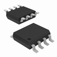
DMS3017SSD-13 Diodes Inc, DMS3017SSD-13 Datasheet

DMS3017SSD-13
Specifications of DMS3017SSD-13
Available stocks
Related parts for DMS3017SSD-13
DMS3017SSD-13 Summary of contents
Page 1
... Device (Note 2) • Qualified to AEC-Q101 Standards for High Reliability Top View Ordering Information (Note 3) Part Number DMS3017SSD-13 Notes purposefully added lead. 2. Diodes Inc.'s "Green" policy can be found on our website at http://www.diodes.com/products/lead_free/index.php. 3. For packaging details our website at http://www.diodes.com/datasheets/ap02007.pdf. Marking Information DMS3017SSD Document number: DS35052 Rev ...
Page 2
... Steady T = 25°C A State T = 70°C A Steady T = 25°C A State T = 70°C A Steady T = 25°C A State T = 70°C A Steady T = 25°C A State T = 70° 25°C (Note 25°C (Note 25° www.diodes.com DMS3017SSD Symbol Value Unit DSS V ±20 V GSS 8 6 7 Symbol ...
Page 3
... 1276 C iss - 160 C oss - 136 C rss - 15.8 t D(on 29.7 t D(off 3 www.diodes.com DMS3017SSD Max Unit Test Condition - 0V 250μ μA 100 V = 30V ±100 ±20V 2 250μ 10V 9. mΩ 4. 15V 0V 1.0MHz - Ω ...
Page 4
... GS 0. 10V 0. 10A D 0.03 0.02 0. 100 125 150 -50 -25 Fig. 6 On-Resistance Variation with Temperature 100 125 150 0 www.diodes.com DMS3017SSD V = 10V 150° 125° 85° 25° -55° DRAIN CURRENT (A) D Fig. 4 Typical On-Resistance vs. Drain Current and Temperature 10V 10A ...
Page 5
... Fig. 9 Typical Total Capacitance 15V 10A TOTAL GATE CHARGE (nC) g Fig. 11 Gate-Charge Characteristics DMS3017SSD Document number: DS35052 Rev 10,000 f = 1MHz 1,000 100 www.diodes.com DMS3017SSD T = 150° 125° 85° 25° DRAIN-SOURCE VOLTAGE (V) DS Fig. 10 Typical Leakage Current vs. Drain-Source Voltage October 2010 © Diodes Incorporated ...
Page 6
... 478.9 C iss - 96.7 C oss - 61.4 C rss - 2.9 t D(on 14.6 t D(off 3 www.diodes.com DMS3017SSD Max Unit Test Condition - 0V 1mA GS D μ 30V ±100 ±20V 2 250μ 10V 8. mΩ 4. 15V 0V 1.0MHz - Ω 0V 0V 1MHz ...
Page 7
... GS 0. 10V 0. 10A D 0.03 0.02 0. 100 125 150 -50 -25 Fig. 17 On-Resistance Variation with Temperature 100 125 150 0 www.diodes.com DMS3017SSD V = 10V 150° 125° 85° 25° -55° DRAIN CURRENT (A) D Fig. 15 Typical On-Resistance vs. Drain Current and Temperature 10V 10A ...
Page 8
... DMS3017SSD Document number: DS35052 Rev 10,000 f = 1MHz 1,000 100 0.9 0.001 0.01 0 PULSE DURATION TIME (s) 1 Fig. 23 Transient Thermal Response www.diodes.com DMS3017SSD T = 150° 125° 85° 25° DRAIN-SOURCE VOLTAGE (V) DS Fig. 21 Typical Leakage Current vs. Drain-Source Voltage R ( θJA θ 113° ...
Page 9
... Suggested Pad Layout DMS3017SSD Document number: DS35052 Rev Gauge Plane A1 Seating Plane L Detail ‘A’ °~ ° ° Detail ‘A’ A3 Dimensions www.diodes.com DMS3017SSD SO-8 Dim Min Max A - 1.75 A1 0.10 0.20 A2 1.30 1.50 A3 0.15 0.25 b 0.3 0.5 D 4.85 4.95 E 5.90 6.10 E1 3.85 3 ...
Page 10
... Diodes Incorporated. Further, Customers must fully indemnify Diodes Incorporated and its representatives against any damages arising out of the use of Diodes Incorporated products in such safety-critical, life support devices or systems. Copyright © 2010, Diodes Incorporated www.diodes.com DMS3017SSD Document number: DS35052 Rev IMPORTANT NOTICE LIFE SUPPORT www.diodes.com DMS3017SSD October 2010 © Diodes Incorporated ...


