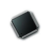
PIC18F86J72-I/PT Microchip Technology, PIC18F86J72-I/PT Datasheet - Page 449

PIC18F86J72-I/PT
Manufacturer Part Number
PIC18F86J72-I/PT
Description
IC PIC MCU 8BIT 14KB FLSH 80TQFP
Manufacturer
Microchip Technology
Series
PIC® 18Fr
Datasheet
1.PIC18F86J72-IPT.pdf
(480 pages)
Specifications of PIC18F86J72-I/PT
Program Memory Type
FLASH
Program Memory Size
64KB (32K x 16)
Package / Case
80-TQFP
Core Processor
PIC
Core Size
8-Bit
Speed
48MHz
Connectivity
I²C, LIN, SPI, UART/USART
Peripherals
Brown-out Detect/Reset, LCD, LVD, POR, PWM, WDT
Number Of I /o
51
Ram Size
3.8K x 8
Voltage - Supply (vcc/vdd)
2 V ~ 3.6 V
Data Converters
A/D 12x12b
Oscillator Type
Internal
Operating Temperature
-40°C ~ 85°C
Data Bus Width
8 bit
Data Ram Size
4 KB
Interface Type
SPI, USART, SPI, I2C
Maximum Clock Frequency
8 MHz
Number Of Programmable I/os
51
Number Of Timers
4
Operating Supply Voltage
2 V to 3.6 V
Maximum Operating Temperature
+ 85 C
Mounting Style
SMD/SMT
Minimum Operating Temperature
- 40 C
On-chip Adc
14
Controller Family/series
PIC18F
No. Of I/o's
51
Ram Memory Size
3923Byte
Cpu Speed
12MIPS
No. Of Timers
4
Rohs Compliant
Yes
Lead Free Status / RoHS Status
Lead free / RoHS Compliant
Lead Free Status / RoHS Status
Lead free / RoHS Compliant, Lead free / RoHS Compliant
Available stocks
Company
Part Number
Manufacturer
Quantity
Price
Company:
Part Number:
PIC18F86J72-I/PT
Manufacturer:
Microchip Technology
Quantity:
10 000
- Current page: 449 of 480
- Download datasheet (5Mb)
B.4.10
The AFE uses an external clock signal to operate its
internal digital logic. An internal clock generation chain
(Figure B-5) is used to produce a range of DRCLK
sampling frequencies.
FIGURE B-5:
B.5
B.5.1
The AFE is accessed for control and data output exclu-
sively through its dedicated Serial Peripheral Interface
(SPI). The interface is compatible with SPI Modes 0,0
and 1,1. Data is clocked out of the AFE on the falling
edge of SCK, and data is clocked in on the rising edge
of SCK. In these modes, SCK can Idle either high or
low.
Each SPI communication starts with a CS falling edge
and stops with the CS rising edge. Each SPI
communication is independent. When CS is high, SDO
is in high-impedance, transitions on SCK and SDI have
no effect. Additional controls pins (ARESET and DR)
are also provided on separate pins for advanced
communication.
The AFE’s SPI interface has a simple command
structure. The first byte transmitted is always the
control byte and is followed by data bytes that are 8-bit
wide. Both ADCs are continuously converting data by
default and can be reset or shut down through a
CONFIG2 register setting.
Since each ADC data is either 16 or 24 bits (depending
on the WIDTH bits), the internal registers can be
grouped together with various configurations (through
the READ bits) in order to allow easy data retrieval
within only one communication. For device reads, the
internal
incremented in order to loop through groups of data
within the register map. SDOA will then output the data
located at the ADDRESS (A<4:0>) defined in the con-
trol byte and then ADDRESS + 1 depending on the
READ<1:0> bits, which select the groups of registers.
These groups are defined in Section B.6.1 “ADC
Channel Data Output Registers” (Register Map).
2010 Microchip Technology Inc.
Serial Interface Description
address
INTERNAL AFE CLOCK
OVERVIEW
CLKIA
AFE INTERNAL CLOCK DETAIL
counter
Digital Buffer
can
MCLK
be
PRESCALE<1:0>
Clock Divider
automatically
Prescale
1/
Preliminary
AMCLK
Clock Divider
PIC18F87J72 FAMILY
1/4
For keeping specified ADC accuracy, AMCLK should
be kept between 1 and 5 MHz with BOOST off, or 1 and
8.192 MHz with BOOST on. Larger MCLK frequencies
can be used provided the prescaler clock settings allow
the AMCLK to respect these ranges.
The Data Ready pin (DR) can be used as an interrupt for
a microcontroller and outputs pulses when new ADC
channel data is available. The ARESET pin acts like a
Hard Reset and can reset the AFE to its default power-up
configuration, independent of the microcontroller.
B.5.2
The control byte of the AFE contains two device
address bits (A<6:5>), 5 register address bits (A<4:0>)
and a read/write bit (R/W). The first byte transmitted to
the AFE is always the control byte.
The AFE interface is device-addressable (through
A<6:5>) so that multiple devices can be present on the
same SPI bus with no data bus contention. This
functionality enables three-phase power metering
systems containing an AFE and two other external
AFE-type chips, controlled by a single SPI bus (single
CS, SCK, SDI and SDO pins). The default device
address bits are ‘00’.
FIGURE B-6:
A read on undefined addresses will give an all zeros
output on the first and all subsequent transmitted bytes.
A write on an undefined address will have no effect and
will not increment the address counter either.
The register map is defined in Section B.6.1 “ADC
Channel Data Output Registers”.
A6
Address
Device
f
Sampling
Rate
DMCLK
S
Bits
ADC
A5 A4
CONTROL BYTE
Clock Divider
OSR<1:0>
CONTROL BYTE
1/OSR
A3 A2
Address Bits
Register
f
Output
Data Rate
DRCLK
D
A1
ADC
DS39979A-page 449
A0
Write Bit
R/W
Read
Related parts for PIC18F86J72-I/PT
Image
Part Number
Description
Manufacturer
Datasheet
Request
R

Part Number:
Description:
Manufacturer:
Microchip Technology Inc.
Datasheet:

Part Number:
Description:
Manufacturer:
Microchip Technology Inc.
Datasheet:

Part Number:
Description:
Manufacturer:
Microchip Technology Inc.
Datasheet:

Part Number:
Description:
Manufacturer:
Microchip Technology Inc.
Datasheet:

Part Number:
Description:
Manufacturer:
Microchip Technology Inc.
Datasheet:

Part Number:
Description:
Manufacturer:
Microchip Technology Inc.
Datasheet:

Part Number:
Description:
Manufacturer:
Microchip Technology Inc.
Datasheet:

Part Number:
Description:
Manufacturer:
Microchip Technology Inc.
Datasheet:


