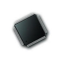
PIC18F86J72-I/PT Microchip Technology, PIC18F86J72-I/PT Datasheet - Page 437

PIC18F86J72-I/PT
Manufacturer Part Number
PIC18F86J72-I/PT
Description
IC PIC MCU 8BIT 14KB FLSH 80TQFP
Manufacturer
Microchip Technology
Series
PIC® 18Fr
Datasheet
1.PIC18F86J72-IPT.pdf
(480 pages)
Specifications of PIC18F86J72-I/PT
Program Memory Type
FLASH
Program Memory Size
64KB (32K x 16)
Package / Case
80-TQFP
Core Processor
PIC
Core Size
8-Bit
Speed
48MHz
Connectivity
I²C, LIN, SPI, UART/USART
Peripherals
Brown-out Detect/Reset, LCD, LVD, POR, PWM, WDT
Number Of I /o
51
Ram Size
3.8K x 8
Voltage - Supply (vcc/vdd)
2 V ~ 3.6 V
Data Converters
A/D 12x12b
Oscillator Type
Internal
Operating Temperature
-40°C ~ 85°C
Data Bus Width
8 bit
Data Ram Size
4 KB
Interface Type
SPI, USART, SPI, I2C
Maximum Clock Frequency
8 MHz
Number Of Programmable I/os
51
Number Of Timers
4
Operating Supply Voltage
2 V to 3.6 V
Maximum Operating Temperature
+ 85 C
Mounting Style
SMD/SMT
Minimum Operating Temperature
- 40 C
On-chip Adc
14
Controller Family/series
PIC18F
No. Of I/o's
51
Ram Memory Size
3923Byte
Cpu Speed
12MIPS
No. Of Timers
4
Rohs Compliant
Yes
Lead Free Status / RoHS Status
Lead free / RoHS Compliant
Lead Free Status / RoHS Status
Lead free / RoHS Compliant, Lead free / RoHS Compliant
Available stocks
Company
Part Number
Manufacturer
Quantity
Price
Company:
Part Number:
PIC18F86J72-I/PT
Manufacturer:
Microchip Technology
Quantity:
10 000
- Current page: 437 of 480
- Download datasheet (5Mb)
The Data Ready pin is independent of the SPI interface
and acts like an interrupt output. The pin state is not
latched and the pulse width (and period) are both deter-
mined by the MCLK frequency, oversampling rate and
internal clock prescale settings. The DR pulse width is
equal to one DMCLK period and the frequency of the
pulses is equal to DRCLK (see Figure 29-22 in
Section 29.0 “Electrical Characteristics” of the data
sheet).
B.2.10
CLKIA provides the master clock for the device. The
typical clock frequency specified is 4 MHz. However,
the clock frequency can be 1 MHz to 5 MHz without
disturbing ADC accuracy. With the current boost circuit
enabled, the master clock can be used up to
8.192 MHz without disturbing ADC accuracy. Appropri-
ate load capacitance should be connected to these
pins for proper operation.
B.2.11
This pin is the SPI chip select that enables the serial
communication.
communication can take place. A chip select falling
edge initiates the serial communication and a chip
select rising edge terminates the communication. No
communication can take place even when CSA is low
and when ARESET is low.
This input is Schmitt triggered.
2010 Microchip Technology Inc.
Note:
MASTER CLOCK INPUT (CLKIA)
This pin should not be left floating when the
DR_HIZN bit is low; a 10 k pull-up resistor
connected to DV
CHIP SELECT (CSA)
When
this
DD
is recommended.
pin
is
high,
Preliminary
no
PIC18F87J72 FAMILY
B.2.12
This is the serial clock pin for SPI communication.
Data is clocked into the device on the rising edge of
SCK. Data is clocked out of the device on the falling
edge of SCK.
The AFE interface is compatible with both SPI 0,0 and
1,1 modes. SPI modes can only be changed during a
Reset.
The maximum clock speed specified is 20 MHz when
SV
This input is Schmitt triggered.
B.2.13
This is the SPI data output pin. Data is clocked out of
the device on the falling edge of SCK.
This pin stays high impedance during the first command
byte. It also stays high impedance during the whole com-
munication for write commands and when the CSA pin
is high or when the ARESET pin is low. This pin is active
only when a read command is processed. Each read is
processed by a packet of 8 bits.
B.2.14
This is the SPI data input pin. Data is clocked into the
device on the rising edge of SCK.
When CS is low, this pin is used to communicate with
series of 8-bit commands.
The interface is half-duplex (inputs and outputs do not
happen at the same time).
Each communication starts with a chip select falling
edge, followed by an 8-bit command word entered
through the SDI pin. Each command is either a read or
a write command. Toggling SDI during a read
command has no effect.
This input is Schmitt triggered.
DD
> 4.5V and 10 MHz otherwise.
SERIAL DATA CLOCK (SCKA)
SERIAL DATA OUTPUT (SDOA)
SERIAL DATA INPUT (SDIA)
DS39979A-page 437
Related parts for PIC18F86J72-I/PT
Image
Part Number
Description
Manufacturer
Datasheet
Request
R

Part Number:
Description:
Manufacturer:
Microchip Technology Inc.
Datasheet:

Part Number:
Description:
Manufacturer:
Microchip Technology Inc.
Datasheet:

Part Number:
Description:
Manufacturer:
Microchip Technology Inc.
Datasheet:

Part Number:
Description:
Manufacturer:
Microchip Technology Inc.
Datasheet:

Part Number:
Description:
Manufacturer:
Microchip Technology Inc.
Datasheet:

Part Number:
Description:
Manufacturer:
Microchip Technology Inc.
Datasheet:

Part Number:
Description:
Manufacturer:
Microchip Technology Inc.
Datasheet:

Part Number:
Description:
Manufacturer:
Microchip Technology Inc.
Datasheet:


