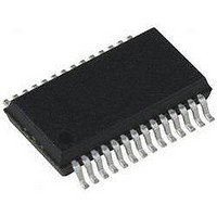
PIC18LF24K22-I/SS Microchip Technology, PIC18LF24K22-I/SS Datasheet - Page 328

PIC18LF24K22-I/SS
Manufacturer Part Number
PIC18LF24K22-I/SS
Description
IC PIC MCU 16KB FLASH 28SSOP
Manufacturer
Microchip Technology
Series
PIC® XLP™ 18Fr
Specifications of PIC18LF24K22-I/SS
Core Size
8-Bit
Program Memory Size
16KB (8K x 16)
Core Processor
PIC
Speed
64MHz
Connectivity
I²C, SPI, UART/USART
Peripherals
Brown-out Detect/Reset, HLVD, POR, PWM, WDT
Number Of I /o
24
Program Memory Type
FLASH
Eeprom Size
256 x 8
Ram Size
768 x 8
Voltage - Supply (vcc/vdd)
1.8 V ~ 3.6 V
Data Converters
A/D 19x10b
Oscillator Type
Internal
Operating Temperature
-40°C ~ 85°C
Package / Case
28-SSOP (0.200", 5.30mm Width)
Controller Family/series
PIC18
No. Of I/o's
25
Eeprom Memory Size
256Byte
Ram Memory Size
768Byte
Cpu Speed
64MHz
No. Of Timers
7
Lead Free Status / RoHS Status
Lead free / RoHS Compliant
- Current page: 328 of 496
- Download datasheet (5Mb)
PIC18(L)F2X/4XK22
19.6
A unique feature on board the CTMU module is its
ability to generate system clock independent output
pulses based on an external capacitor value. This is
accomplished using the internal comparator voltage
reference module, Comparator 2 input pin and an
external capacitor. The pulse is output onto the CTPLS
pin. To enable this mode, set the TGEN bit.
See
chosen by the user to determine the output pulse width
on CTPLS. The pulse width is calculated by
T = (C
source measurement step
Source
voltage (CV
FIGURE 19-4:
19.7
19.7.1
When the device enters any Sleep mode, the CTMU
module current source is always disabled. If the CTMU
is performing an operation that depends on the current
source when Sleep mode is invoked, the operation may
not
measurements may return erroneous values.
DS41412D-page 328
Figure 19-4
terminate
PULSE
Calibration”) and V is the internal reference
Creating a Delay with the CTMU
Module
Operation During Sleep/Idle
Modes
/I)*V, where I is known from the current
REF
SLEEP MODE AND DEEP SLEEP
MODES
).
correctly.
for an example circuit. C
TYPICAL CONNECTIONS AND INTERNAL CONFIGURATION FOR PULSE
DELAY GENERATION
C12IN1-
C
CTED1
(Section 19.3.1 “Current
PULSE
Capacitance
and
PULSE
PIC18(L)FXXK22 Device
EDG1
time
Preliminary
CV
is
Current Source
REF
Comparator
CTMU
C2
An example use of this feature is for interfacing with
variable capacitive-based sensors, such as a humidity
sensor. As the humidity varies, the pulse width output
on CTPLS will vary. The CTPLS output pin can be con-
nected to an input capture pin and the varying pulse
width is measured to determine the humidity in the
application.
Follow these steps to use this feature:
1.
2.
3.
4.
5.
19.7.2
The behavior of the CTMU in Idle mode is determined
by the CTMUSIDL bit (CTMUCONH<5>). If CTMUSIDL
is cleared, the module will continue to operate in Idle
mode. If CTMUSIDL is set, the module’s current source
is disabled when the device enters Idle mode. If the
module is performing an operation when Idle mode is
invoked, in this case, the results will be similar to those
with Sleep mode.
19.8
When this peripheral is not used, the Peripheral
Module Disable bit can be set to disconnect all clock
sources to the module, reducing power consumption to
an absolute minimum. See
Peripheral Module
Initialize Comparator 2.
Initialize the comparator voltage reference.
Initialize the CTMU and enable time delay
generation by setting the TGEN bit.
Set EDG1STAT.
When C
reference trip point, an output pulse is generated
on CTPLS.
CTMU Peripheral Module Disable
(PMD)
IDLE MODE
PULSE
charges to the value of the voltage
Control”.
CTPLS
2010 Microchip Technology Inc.
Section 3.6 “Selective
Related parts for PIC18LF24K22-I/SS
Image
Part Number
Description
Manufacturer
Datasheet
Request
R

Part Number:
Description:
Manufacturer:
Microchip Technology Inc.
Datasheet:

Part Number:
Description:
Manufacturer:
Microchip Technology Inc.
Datasheet:

Part Number:
Description:
Manufacturer:
Microchip Technology Inc.
Datasheet:

Part Number:
Description:
Manufacturer:
Microchip Technology Inc.
Datasheet:

Part Number:
Description:
Manufacturer:
Microchip Technology Inc.
Datasheet:

Part Number:
Description:
Manufacturer:
Microchip Technology Inc.
Datasheet:

Part Number:
Description:
Manufacturer:
Microchip Technology Inc.
Datasheet:

Part Number:
Description:
Manufacturer:
Microchip Technology Inc.
Datasheet:


