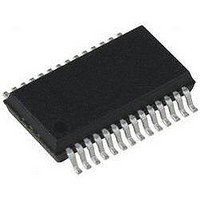
PIC18LF24K22-I/SS Microchip Technology, PIC18LF24K22-I/SS Datasheet - Page 291

PIC18LF24K22-I/SS
Manufacturer Part Number
PIC18LF24K22-I/SS
Description
IC PIC MCU 16KB FLASH 28SSOP
Manufacturer
Microchip Technology
Series
PIC® XLP™ 18Fr
Specifications of PIC18LF24K22-I/SS
Core Size
8-Bit
Program Memory Size
16KB (8K x 16)
Core Processor
PIC
Speed
64MHz
Connectivity
I²C, SPI, UART/USART
Peripherals
Brown-out Detect/Reset, HLVD, POR, PWM, WDT
Number Of I /o
24
Program Memory Type
FLASH
Eeprom Size
256 x 8
Ram Size
768 x 8
Voltage - Supply (vcc/vdd)
1.8 V ~ 3.6 V
Data Converters
A/D 19x10b
Oscillator Type
Internal
Operating Temperature
-40°C ~ 85°C
Package / Case
28-SSOP (0.200", 5.30mm Width)
Controller Family/series
PIC18
No. Of I/o's
25
Eeprom Memory Size
256Byte
Ram Memory Size
768Byte
Cpu Speed
64MHz
No. Of Timers
7
Lead Free Status / RoHS Status
Lead free / RoHS Compliant
- Current page: 291 of 496
- Download datasheet (5Mb)
17.0
The
conversion of an analog input signal to a 10-bit binary
representation of that signal. This device uses analog
inputs, which are multiplexed into a single sample and
hold circuit. The output of the sample and hold is
connected to the input of the converter. The converter
generates a 10-bit binary result via successive
approximation and stores the conversion result into the
ADC result registers (ADRESL and ADRESH).
FIGURE 17-1:
2010 Microchip Technology Inc.
Note: Additional ADC channels AN5-AN7 and AN20-AN27 are only available on PIC18(L)F4XK22 devices.
Analog-to-Digital
ANALOG-TO-DIGITAL
CONVERTER (ADC) MODULE
V
V
REF
REF
AN28
AN27
AN5
+/AN3
FVR BUF2
FVR BUF2
-/AN2
Reserved
AN4
Reserved
Reserved
AN3
AN2
AN1
AN0
Reserved
(1)
(1)
ADC BLOCK DIAGRAM
(1)
CTMU
A
A
VDD
VSS
Converter
11101
11100
11011
11111
11110
00101
00100
00011
00010
00001
00000
11
11
10
10
00
01
00
01
(ADC)
2
2
5
allows
Preliminary
PVCFG<1:0>
NVCFG<1:0>
CHS<4:0>
The ADC voltage reference is software selectable to
either V
pins.
The ADC can generate an interrupt upon completion of
a conversion. This interrupt can be used to wake-up the
device from Sleep.
Figure 17-1
10-Bit ADC
PIC18(L)F2X/4XK22
DD
or a voltage applied to the external reference
shows the block diagram of the ADC.
ADFM
10
ADCMD
GO/DONE
ADON
ADRESH
0 = Left Justify
1 = Right Justify
10
DS41412D-page 291
ADRESL
Related parts for PIC18LF24K22-I/SS
Image
Part Number
Description
Manufacturer
Datasheet
Request
R

Part Number:
Description:
Manufacturer:
Microchip Technology Inc.
Datasheet:

Part Number:
Description:
Manufacturer:
Microchip Technology Inc.
Datasheet:

Part Number:
Description:
Manufacturer:
Microchip Technology Inc.
Datasheet:

Part Number:
Description:
Manufacturer:
Microchip Technology Inc.
Datasheet:

Part Number:
Description:
Manufacturer:
Microchip Technology Inc.
Datasheet:

Part Number:
Description:
Manufacturer:
Microchip Technology Inc.
Datasheet:

Part Number:
Description:
Manufacturer:
Microchip Technology Inc.
Datasheet:

Part Number:
Description:
Manufacturer:
Microchip Technology Inc.
Datasheet:


