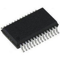
PIC18LF24K22-I/SS Microchip Technology, PIC18LF24K22-I/SS Datasheet - Page 151

PIC18LF24K22-I/SS
Manufacturer Part Number
PIC18LF24K22-I/SS
Description
IC PIC MCU 16KB FLASH 28SSOP
Manufacturer
Microchip Technology
Series
PIC® XLP™ 18Fr
Specifications of PIC18LF24K22-I/SS
Core Size
8-Bit
Program Memory Size
16KB (8K x 16)
Core Processor
PIC
Speed
64MHz
Connectivity
I²C, SPI, UART/USART
Peripherals
Brown-out Detect/Reset, HLVD, POR, PWM, WDT
Number Of I /o
24
Program Memory Type
FLASH
Eeprom Size
256 x 8
Ram Size
768 x 8
Voltage - Supply (vcc/vdd)
1.8 V ~ 3.6 V
Data Converters
A/D 19x10b
Oscillator Type
Internal
Operating Temperature
-40°C ~ 85°C
Package / Case
28-SSOP (0.200", 5.30mm Width)
Controller Family/series
PIC18
No. Of I/o's
25
Eeprom Memory Size
256Byte
Ram Memory Size
768Byte
Cpu Speed
64MHz
No. Of Timers
7
Lead Free Status / RoHS Status
Lead free / RoHS Compliant
- Current page: 151 of 496
- Download datasheet (5Mb)
TABLE 10-16: CONFIGURATION REGISTERS ASSOCIATED WITH PORTE
10.7
Most port pins are multiplexed with analog functions
such
comparators. When these I/O pins are to be used as
analog inputs it is necessary to disable the digital input
buffer to avoid excessive current caused by improper
biasing of the digital input. Individual control of the
digital input buffers on pins which share analog
functions is provided by the ANSELA, ANSELB,
ANSELC, ANSELD and ANSELE registers. Setting an
ANSx bit high will disable the associated digital input
buffer and cause all reads of that pin to return ‘0’ while
allowing analog functions of that pin to operate
correctly.
The state of the ANSx bits has no affect on digital
output functions. A pin with the associated TRISx bit
clear and ANSx bit set will still operate as a digital
output but the input mode will be analog. This can
cause unexpected behavior when performing read-
modify-write operations on the affected port.
All ANSEL register bits default to ‘1’ upon POR and
BOR, disabling digital inputs for their associated port
pins. All TRIS register bits default to ‘1’ upon POR or
BOR, disabling digital outputs for their associated port
pins. As a result, all port pins that have an ANSEL
register will default to analog inputs upon POR or BOR.
REGISTER 10-1:
2010 Microchip Technology Inc.
CONFIG3H
CONFIG4L
Legend: — = unimplemented locations, read as ‘0’. Shaded bits are not used for Interrupts.
Note 1:
bit 7
Legend:
R = Readable bit
‘1’ = Bit is set
-n/n = Value at POR and BOR/Value at all other Resets
bit 7-0
Note 1:
Name
R/W-u/x
Rx7
2:
as
Port Analog Control
Can only be changed when in high voltage programming mode.
Register Description for PORTA, PORTB, PORTC and PORTD.
Writes to PORTx are written to corresponding LATx register. Reads from PORTx register is return of I/O
pin values.
the
MCLRE
DEBUG
Rx<7:0>: PORTx I/O bit values
Bit 7
Analog-to-Digital
R/W-u/x
Rx6
PORTX
XINST
Bit 6
—
W = Writable bit
‘0’ = Bit is cleared
(1)
R/W-u/x
: PORTx REGISTER
Rx5
Converter
P2BMX
Bit 5
—
(2)
R/W-u/x
Rx4
T3CMX
and
Preliminary
Bit 4
—
U = Unimplemented bit, read as ‘0’
x = Bit is unknown
HFOFST CCP3MX PBADEN CCP2MX
R/W-u/x
10.8
The output slew rate of each port is programmable to
select either the standard transition rate or a reduced
transition rate of approximately 0.1 times the standard
to minimize EMI. The reduced transition time is the
default slew rate for all ports.
Bit 3
Rx3
—
PIC18(L)F2X/4XK22
Port Slew Rate Control
LVP
Bit 2
R/W-u/x
(1)
Rx2
Bit 1
—
R/W-u/x
Rx1
STRVEN
Bit 0
DS41412D-page 151
R/W-u/x
on page
Rx0
Values
Reset
354
355
bit 0
Related parts for PIC18LF24K22-I/SS
Image
Part Number
Description
Manufacturer
Datasheet
Request
R

Part Number:
Description:
Manufacturer:
Microchip Technology Inc.
Datasheet:

Part Number:
Description:
Manufacturer:
Microchip Technology Inc.
Datasheet:

Part Number:
Description:
Manufacturer:
Microchip Technology Inc.
Datasheet:

Part Number:
Description:
Manufacturer:
Microchip Technology Inc.
Datasheet:

Part Number:
Description:
Manufacturer:
Microchip Technology Inc.
Datasheet:

Part Number:
Description:
Manufacturer:
Microchip Technology Inc.
Datasheet:

Part Number:
Description:
Manufacturer:
Microchip Technology Inc.
Datasheet:

Part Number:
Description:
Manufacturer:
Microchip Technology Inc.
Datasheet:


