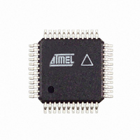
AT86RF211DAI-R Atmel, AT86RF211DAI-R Datasheet - Page 17

AT86RF211DAI-R
Manufacturer Part Number
AT86RF211DAI-R
Description
IC TXRX FR FSK 400-950MHZ 48-TQF
Manufacturer
Atmel
Datasheet
1.AT86RF211DAI-R.pdf
(48 pages)
Specifications of AT86RF211DAI-R
Frequency
400MHz ~ 950MHz
Data Rate - Maximum
100kbps
Modulation Or Protocol
FSK
Applications
ISM
Power - Output
7dBm ~ 12dBm
Sensitivity
-107dBm
Voltage - Supply
2.4 V ~ 3.6 V
Data Interface
PCB, Surface Mount
Antenna Connector
PCB, Surface Mount
Operating Temperature
-40°C ~ 85°C
Package / Case
48-TQFP Exposed Pad, 48-eTQFP, 48-HTQFP, 48-VQFP
Lead Free Status / RoHS Status
Contains lead / RoHS non-compliant
Memory Size
-
Current - Transmitting
-
Current - Receiving
-
Data Slicer
1942C–WIRE–06/02
The input RBW resistor controls the discriminator bandwidth. This bandwidth is selected
by CTRL1[6]. The default value is "standard discriminator BW". The slope of the discrim-
inator increases by 5 mV/kHz/V with V
Example:
The analog signals at the output of the discriminator (DISCOUT, pin 27) are converted
into CMOS level data by a high resolution comparator called a Data Slicer.
The Data Slicer has a reference for its comparator which can be chosen thanks to
CTRL1[4]. The reference sets the comparison level of the comparator. One option is to
extract the average value of the demodulated signal on the SKFILT pin (25), this is the
external mode. The other option is to set an absolute value for this reference (internal
mode).
•
The external mode uses the average value of the demodulated signal as the compari-
son level for the comparator. Thus there must be enough transitions in the message to
ensure that the average value remains between the "0" level and the "1" level. Manches-
ter encoding can be used in this mode as well as DC-free encoding schemes. The
choice for SKFILT capacitor is a trade-off between the maximum duration of a constant
bit (whatever "0" or "1") and the max allowed settling time to charge this capacitor after
powering up.
Note:
•
The internal mode uses the output of a DAC as the comparison level. Once this thres-
hold has been correctly set, an "absolute" data slicing of the demodulated signal is
possible: no need for DC-free modulation scheme (it is possible to send a "0" or "1"
infinitely).
Figure 21. Schematic of the Data Slicer
External mode:
Internal mode:
V
V
CC
CC
The SKFILT pin is in high impedance state during the "sleep" period of the Wake Up
mode, so that the level is kept constant and there is no need to charge again this tank.
= 3V implies +17 mV/kHz sensitivity for the demodulator
= 3.6V implies +20 mV/kHz sensitivity for the demodulator
Choice of internal or
external reference for
the data slicer
DATAMSG
+
-
CC
Vdd/2
and is 14 mV at 2.4V.
+
-
+
Σ
+
-
+
100 kΩ
4 bits
SKFILT
DSIN
DISCOUT
AT86RF211
17


