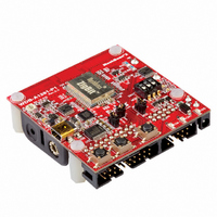
MNZB-24-B0 MeshNetics, MNZB-24-B0 Datasheet - Page 9

MNZB-24-B0
Manufacturer Part Number
MNZB-24-B0
Description
MOD 802.15.4/ZIGB 2.4GHZ RF PORT
Manufacturer
MeshNetics
Series
Zigbit™r
Datasheet
1.MNZB-24-B0.pdf
(24 pages)
Specifications of MNZB-24-B0
Frequency
2.4GHz
Data Rate - Maximum
250kbps
Modulation Or Protocol
802.15.4 Zigbee
Power - Output
3dBm
Sensitivity
-101dBm
Voltage - Supply
1.8 V ~ 3.6 V
Current - Receiving
19mA
Current - Transmitting
18mA
Data Interface
PCB, Surface Mount
Memory Size
128kBytes Flash, 8kBytes RAM, 4kBytes EEPROM
Antenna Connector
PCB, Surface Mount
Operating Temperature
-40°C ~ 85°C
Package / Case
Module
Lead Free Status / RoHS Status
Lead free / RoHS Compliant
Applications
-
Other names
758-1000-2
ZDM-A1281-B0
ZDM-A1281-B0
© 2007 MeshNetics
Connector
9, 22, 23
24, 25
Pin
10
11
12
13
14
15
16
17
18
19
20
21
26
27
28
29
30
31
32
33
34
1
2
3
4
5
6
7
8
Pin Name
SPI_CLK
SPI_MISO
SPI_MOSI
GPIO0
GPIO1
GPIO2
OSC32K_OUT
RESET
DGND
CPU_CLK
I2C_CLK
I2C_DATA
UART_TXD
UART_RXD
UART_RTS
UART_CTS
GPIO6
GPIO7
GPIO3
GPIO4
GPIO5
D_VCC
JTAG_TMS
JTAG_TDI
JTAG_TDO
JTAG_TCK
ADC_INPUT_3
ADC_INPUT_2
ADC_INPUT_1
BAT
A_VREF
Description
Reserved for stack operation
Reserved for stack operation
Reserved for stack operation
General purpose digital input/output 0
General purpose digital input/output 1
General purpose digital input/output 2
32.768 kHz clock output.
Reset input (active low).
Digital ground
RF clock output. When module is in
active state, 4 MHz signal is present on
this line. While module is in the sleeping
state, clock generation is stopped also.
I
I
UART receive input
UART transmit output
RTS input (Request To Send) for UART
hardware flow control. Active low.
CTS output (Clear To Send) for UART
hardware flow control. Active low.
General purpose digital input/output 6
General purpose digital input/output 7
General purpose digital input/output 3
General purpose digital input/output 4
General purpose digital input/output 5
Digital supply voltage (V
JTAG test mode select
JTAG test data input
JTAG test data output
JTAG test clock
ADC input channel 3
ADC input channel 2
ADC input channel 1
ADC input channel 0. Used by the stack
for battery level measurement. Nominal
voltage to AGND is 1 V .
Output/Input reference voltage for ADC
2
2
C serial clock output
C serial data input/output
Zi gBi t™ O EM M odule s
cc
)
I/O
I/O
I/O
I/O
I/O
I/O
I/O
I/O
I/O
I/O
I/O
I/O
I/O
O
O
O
O
O
O
O
I
I
I
I
I
I
I
I
I
I
power on
Default
tri-state
tri-state
tri-state
tri-state
tri-state
tri-state
tri-state
tri-state
tri-state
tri-state
tri-state
tri-state
tri-state
tri-state
tri-state
tri-state
tri-state
tri-state
tri-state
Pin Assignment Table
State
after
Product Datasheet
Notes,
see the
list
below
3
3
3
1, 2, 3, 6
1, 2, 3, 6
1, 2, 3, 6
3, 4
3
3
1, 2, 3, 6
1, 2, 3, 6
1, 2, 3, 6
1, 2, 3, 6
1, 2, 3, 6
1, 2, 3, 6,
7
1, 2, 3, 6
1, 2, 3, 6
1, 2, 3, 6
1, 2, 3, 6
1, 2, 3, 6
8
1, 2, 3, 5
1, 2, 3, 5
1, 2, 3, 5
1, 2, 3, 5
1, 2, 6
1, 2, 6
1, 2, 6
1, 2, 6
Page 9 of 24


