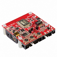
MNZB-24-B0 MeshNetics, MNZB-24-B0 Datasheet - Page 10

MNZB-24-B0
Manufacturer Part Number
MNZB-24-B0
Description
MOD 802.15.4/ZIGB 2.4GHZ RF PORT
Manufacturer
MeshNetics
Series
Zigbit™r
Datasheet
1.MNZB-24-B0.pdf
(24 pages)
Specifications of MNZB-24-B0
Frequency
2.4GHz
Data Rate - Maximum
250kbps
Modulation Or Protocol
802.15.4 Zigbee
Power - Output
3dBm
Sensitivity
-101dBm
Voltage - Supply
1.8 V ~ 3.6 V
Current - Receiving
19mA
Current - Transmitting
18mA
Data Interface
PCB, Surface Mount
Memory Size
128kBytes Flash, 8kBytes RAM, 4kBytes EEPROM
Antenna Connector
PCB, Surface Mount
Operating Temperature
-40°C ~ 85°C
Package / Case
Module
Lead Free Status / RoHS Status
Lead free / RoHS Compliant
Applications
-
Other names
758-1000-2
ZDM-A1281-B0
ZDM-A1281-B0
Notes:
© 2007 MeshNetics
Connector
44, 46, 48
1.
2.
3.
4.
5.
6.
7.
8.
Pin
35
36
37
38
39
40
41
42
43
45
47
Most of pins can be configured for general purpose I/O or for some alternate functions as described in
details in the ATmega1281V Datasheet [1].
GPIO pins can be programmed either for output, or for input with/without pull-up resistors. Output pin
drivers are strong enough to drive LED displays directly (refer to figures on pages 387-388, [1]).
All digital pins are provided with protection diodes to D_VCC and DGND
It is strongly recommended to avoid assigning an alternate function for OSC32K_OUT pin because it is
used by eZeeNet Framework. However, this signal can be used if another peripheral or host processor
requires 32.768 kHz clock, otherwise this pin can be disconnected.
Normally, JTAG_TMS, JTAG_TDI, JTAG_TDO, JTAG_TCK pins are used for on-chip debugging and flash
burning. They can be used for A/D conversion if JTAGEN fuse is disabled.
eZeeNet software can configure the following pins to be general-purpose I/O lines: GPIO0, GPIO1, GPIO2,
GPIO3, GPIO4, GPIO5, GPIO6, GPIO7, GPIO8, GPIO_1WR, I2C_CLK, I2C_DATA, UART_TXD,
UART_RXD,
UART_DTR, USART0_RXD, USART0_TXD, USART0_EXTCLK, IRQ_7, IRQ_6. Additionally, four JTAG
lines can be programmed with software as GPIO as well, but this requires changing the fuse bits and will
disable JTAG debugging.
With eZeeNet, CTS pin can be configured to indicate sleep/active condition of the module thus providing
mechanism for power management of host processor. If this function is necessary, connection of this pin to
external pull-down resistor is recommended to prevent the undesirable transients during module reset
process.
Using ferrite bead and 1 µF capacitor located closely to the power supply pin is recommended, as shown
below.
Pin Name
AGND
GPIO_1WR
UART_DTR
USART0_RXD
USART0_TXD
USART0_EXTCLK
GPIO8
IRQ_7
IRQ_6
RF_GND
RFP_IO
RFN_IO
UART_RTS,
Description
Analog ground
1-Wire Interface
DTR input (Data Terminal Ready) for
UART. Active low.
UART/SPI receive pin
UART/SPI transmit pin
UART/SPI external clock
General purpose digital input/output 8
Digital input interrupt request 7
Digital input interrupt request 6
RF analog ground
Differential RF input/output.
Differential RF input/output.
UART_CTS,
1,8...3,6 V
Zi gBi t™ O EM M odule s
ADC_INPUT_3,
D_VCC
DGND
ADC_INPUT_2,
I/O
I/O
I/O
I/O
I/O
O
I
I
I
I
I
power on
Default
tri-state
tri-state
tri-state
tri-state
tri-state
tri-state
tri-state
State
after
ADC_INPUT_1,
Product Datasheet
Page 10 of 24
Notes,
see the
list
below
1, 2, 3, 6
1, 2, 3, 6
1, 2, 3, 6
1, 2, 3, 6
1, 2, 3, 6
1, 2, 3, 6
1, 2, 3, 6
1, 2, 3, 6
9
9
9
BAT,


