SX1212IWLTRT Semtech, SX1212IWLTRT Datasheet - Page 2
SX1212IWLTRT
Manufacturer Part Number
SX1212IWLTRT
Description
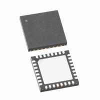
IC TXRX 300MHZ-510MHZ 32-TQFN
Manufacturer
Semtech
Datasheet
1.SX1212IWLTRT.pdf
(77 pages)
Specifications of SX1212IWLTRT
Frequency
300MHz ~ 510MHz
Data Rate - Maximum
150kbps
Modulation Or Protocol
FSK, OOK
Applications
AMR, ISM, Home Automation, Process Control
Power - Output
12.5dBm
Sensitivity
-110dBm
Voltage - Supply
2.1 V ~ 3.6 V
Current - Receiving
3mA
Current - Transmitting
25mA
Data Interface
PCB, Surface Mount
Antenna Connector
PCB, Surface Mount
Operating Temperature
-40°C ~ 85°C
Package / Case
32-TQFN
Operating Temperature (min)
-40C
Operating Temperature (max)
85C
Operating Temperature Classification
Industrial
Modulation Type
FSK/OOK
Package Type
TQFN EP
Operating Supply Voltage (min)
2.1V
Operating Supply Voltage (typ)
2.5/3.3V
Operating Supply Voltage (max)
3.6V
Lead Free Status / RoHS Status
Lead free / RoHS Compliant
Memory Size
-
Lead Free Status / Rohs Status
Supplier Unconfirmed
Other names
SX1212IWLTR
Available stocks
Company
Part Number
Manufacturer
Quantity
Price

Part Number:
SX1212IWLTRT
Manufacturer:
SEMTECH/美国升特
Quantity:
20 000


Table of Contents
1. General Description ................................................................... 5
2. Electrical Characteristics............................................................ 8
3. Architecture Description ........................................................... 12
4. Operating Modes...................................................................... 33
5. Data Processing....................................................................... 34
Rev 2 – June 18th, 2009
ADVANCED COMMUNICATIONS & SENSING
1.1. Simplified Block Diagram................................................... 5
1.2. Pin Diagram ....................................................................... 6
1.3. Pin Description................................................................... 7
2.1. ESD Notice ........................................................................ 8
2.2. Absolute Maximum Ratings ............................................... 8
2.3. Operating Range ............................................................... 8
2.4. Chip Specification .............................................................. 8
3.1. Power Supply Strategy .................................................... 12
3.2. Frequency Synthesis Description .................................... 13
3.3. Transmitter Description ................................................... 18
3.4. Receiver Description........................................................ 23
4.1. Modes of Operation ......................................................... 33
4.2. Digital Pin Configuration vs. Chip Mode .......................... 33
5.1. Overview.......................................................................... 34
5.2. Control Block Description ................................................ 35
2.4.1. Power Consumption .................................................. 8
2.4.2. Frequency Synthesis................................................. 9
2.4.3. Transmitter ................................................................ 9
2.4.4. Receiver .................................................................. 10
2.4.5. Digital Specification ................................................. 11
3.2.1. Reference Oscillator................................................ 13
3.2.2. CLKOUT Output ...................................................... 13
3.2.3. PLL Architecture...................................................... 14
3.2.4. PLL Tradeoffs.......................................................... 14
3.2.5. Voltage Controlled Oscillator................................... 15
3.2.6. PLL Loop Filter ........................................................ 16
3.2.7. PLL Lock Detection Indicator .................................. 16
3.2.8. Frequency Calculation ............................................ 16
3.3.1. Architecture Description .......................................... 18
3.3.2. Bit Rate Setting ....................................................... 19
3.3.3. Alternative Settings ................................................. 19
3.3.4. Fdev Setting in FSK Mode ...................................... 19
3.3.5. Fdev Setting in OOK Mode ..................................... 19
3.3.6. Interpolation Filter ................................................... 20
3.3.7. Power Amplifier ....................................................... 20
3.3.8. Common Input and Output Front-End..................... 22
3.4.1. Architecture ............................................................. 23
3.4.2. LNA and First Mixer ................................................ 24
3.4.3. IF Gain and Second I/Q Mixer................................. 24
3.4.4. Channel Filters ........................................................ 24
3.4.5. Channel Filters Setting in FSK Mode ...................... 25
3.4.6. Channel Filters Setting in OOK Mode ..................... 26
3.4.7. RSSI ........................................................................ 26
3.4.8. Fdev Setting in Receive Mode ................................ 28
3.4.9. FSK Demodulator.................................................... 28
3.4.10. OOK Demodulator................................................. 28
3.4.11. Bit Synchronizer .................................................... 31
3.4.12. Alternative Settings ............................................... 32
3.4.13. Data Output ........................................................... 32
5.1.1. Block Diagram ......................................................... 34
5.1.2. Data Operation Modes ............................................ 34
5.2.1. SPI Interface ........................................................... 35
5.2.2. FIFO ........................................................................ 38
5.2.3. Sync Word Recognition........................................... 39
5.2.4. Packet Handler........................................................ 40
Page 2 of 77
6. Configuration and Status Registers ..........................................58
7. Application Information .............................................................66
8. Packaging Information ..............................................................75
9. Revision History ........................................................................77
10. Contact Information.................................................................77
5.3. Continuous Mode .............................................................41
5.4. Buffered Mode ..................................................................44
5.5. Packet Mode.....................................................................49
6.1. General Description..........................................................58
6.2. Main Configuration Register - MCParam..........................58
6.3. Interrupt Configuration Parameters - IRQParam ..............60
6.4. Receiver Configuration parameters - RXParam ...............62
6.5. Sync Word Parameters - SYNCParam.............................63
6.6. Transmitter Parameters - TXParam .................................64
6.7. Oscillator Parameters - OSCParam .................................64
6.8. Packet Handling Parameters – PKTParam ......................65
7.1. Crystal Resonator Specification .......................................66
7.2. Software for Frequency Calculation .................................66
7.3. Switching Times and Procedures .....................................66
7.4. Reset of the Chip..............................................................72
7.5. Reference Design.............................................................73
8.1. Package Outline Drawing .................................................75
8.2. PCB Land Pattern.............................................................75
8.3. Tape & Reel Specification ................................................76
5.2.5. Control......................................................................40
5.3.1. General Description .................................................41
5.3.2. Tx Processing ..........................................................41
5.3.3. Rx Processing ..........................................................42
5.3.4. Interrupt Signals Mapping ........................................42
5.3.5. uC Connections........................................................43
5.3.6. Continuous Mode Example ......................................43
5.4.1. General Description .................................................44
5.4.2. Tx Processing ..........................................................44
5.4.3. Rx Processing ..........................................................45
5.4.4. Interrupt Signals Mapping ........................................46
5.4.5. uC Connections........................................................47
5.4.6. Buffered Mode Example...........................................47
5.5.1. General Description .................................................49
5.5.2. Packet Format..........................................................49
5.5.3. Tx Processing ..........................................................51
5.5.4. Rx Processing ..........................................................51
5.5.5. Packet Filtering ........................................................52
5.5.6. DC-Free Data Mechanisms......................................53
5.5.7. Interrupt Signal Mapping ..........................................54
5.5.8. uC Connections........................................................55
5.5.9. Packet Mode Example .............................................56
5.5.10. Additional Information ............................................56
7.2.1. GUI ...........................................................................66
7.2.2. .dll for Automatic Production Bench .........................66
7.3.1. Optimized Receive Cycle .........................................67
7.3.2. Optimized Transmit Cycle ........................................68
7.3.3. Transmitter Frequency Hop Optimized Cycle ..........69
7.3.4. Receiver Frequency Hop Optimized Cycle ..............70
7.3.5. Rx Tx and Tx Rx Jump Cycles............................71
7.4.1. POR .........................................................................72
7.4.2. Manual Reset ...........................................................72
7.5.1. Application Schematic..............................................73
7.5.2. PCB Layout ..............................................................73
7.5.3. Bill Of Material..........................................................74
www.semtech.com
SX1212
Related parts for SX1212IWLTRT
Image
Part Number
Description
Manufacturer
Datasheet
Request
R

Part Number:
Description:
EVALUATION BOARD
Manufacturer:
Semtech
Datasheet:
Part Number:
Description:
EVALUATION BOARD
Manufacturer:
Semtech
Datasheet:
Part Number:
Description:
VOLTAGE SUPPRESSOR, TRANSIENT SEMTECH
Manufacturer:
Semtech
Datasheet:

Part Number:
Description:
HIGH VOLTAGE CAPACITORS MONOLITHIC CERAMIC TYPE
Manufacturer:
Semtech Corporation
Datasheet:
Part Number:
Description:
EZ1084CM5.0 AMP POSITIVE VOLTAGE REGULATOR
Manufacturer:
Semtech Corporation
Datasheet:
Part Number:
Description:
3.0 AMP LOW DROPOUT POSITIVE VOLTAGE REGULATORS
Manufacturer:
Semtech Corporation
Datasheet:
Part Number:
Description:
Manufacturer:
Semtech Corporation
Datasheet:
Part Number:
Description:
RailClamp Low Capacitance TVS Diode Array
Manufacturer:
Semtech Corporation
Datasheet:
Part Number:
Description:
Manufacturer:
Semtech Corporation
Datasheet:
Part Number:
Description:
Manufacturer:
Semtech Corporation
Datasheet:
Part Number:
Description:
Manufacturer:
Semtech Corporation
Datasheet:
Part Number:
Description:
Manufacturer:
Semtech Corporation
Datasheet: