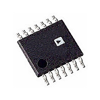
AD8343ARU-REEL Analog Devices Inc, AD8343ARU-REEL Datasheet - Page 18

AD8343ARU-REEL
Manufacturer Part Number
AD8343ARU-REEL
Description
IC MIXER ACTIVE HI-IP3 14-TSSOP
Manufacturer
Analog Devices Inc
Series
AD8343r
Datasheet
1.AD8343ARUZ.pdf
(32 pages)
Specifications of AD8343ARU-REEL
Rohs Status
RoHS non-compliant
Rf Type
Cellular, WLAN
Frequency
0Hz ~ 2.5GHz
Number Of Mixers
1
Gain
7dB
Noise Figure
14dB
Secondary Attributes
Up/Down Converter
Current - Supply
60mA
Voltage - Supply
4.5 V ~ 5.5 V
Package / Case
14-TSSOP (0.173", 4.40mm Width)
Operating Temperature (min)
-40C
Operating Temperature (max)
85C
Operating Temperature Classification
Industrial
Lead Free Status / Rohs Status
Not Compliant
Available stocks
Company
Part Number
Manufacturer
Quantity
Price
AD8343
INPUT INTERFACE (INPP AND INPM)
SINGLE-ENDED-TO-DIFFERENTIAL CONVERSION
The AD8343 is designed to accept differential input signals for
best performance. While a single-ended input can be applied,
the signal capacity is reduced by 6 dB. Furthermore, there is no
cancellation of even-order distortion arising from the nonlinear
input impedances, so the effective signal handling capacity is
reduced even further in distortion-sensitive situations. That is,
the intermodulation intercepts are degraded.
For these reasons, it is strongly recommended that differ
ential signals be presented to the AD8343’s input. In addition
to commercially available baluns, there are various discrete and
printed circuit networks that can produce the required balanced
waveforms and impedance match. These alternate circuits can
be employed to possibly reduce the component cost of the
mixer and/or improve performance.
Baluns implemented in transmission line form (also known as
common-mode chokes) are useful up to frequencies of around
1 GHz to 2 GHz, but are often excessively lossy at the higher
frequencies that the AD8343 can handle. M/A-COM manufac-
tures these baluns and Murata produces a true surface-mount
balun. Coilcraft® and Toko are also manufacturers of RF baluns.
INPUT MATCHING CONSIDERATIONS
The design of the input matching network must be undertaken
with two goals in mind: matching the source impedance to the
input impedance of the AD8343 and providing a dc bias current
path for the bias setting resistors.
The maximum power transfer into the device occurs when
there is a conjugate impedance match between the signal source
and the input of the AD8343. This match is achieved with the
differential equivalent of the classic L network, as illustrated in
Figure 56. The figure gives two examples of the transformation
from a single-ended L network to its differential counterpart.
The design of L matching networks is adequately covered in
texts on RF amplifier design (for example, Microwave Transistor
Amplifiers by Guillermo Gonzalez).
Figure 57 shows the differential input impedance of the
AD8343 at the pins of the device. The two measurements
shown in the figure are for two different core currents set by
Resistor R3 and Resistor R4; the real value impedance shift is
Figure 56. Single-Ended-to-Differential Transformation
SINGLE-ENDED
L1
L2
C2
C1
DIFFERENTIAL
L1/2
L1/2
L2
2C2
2C2
C1
Rev. B | Page 18 of 32
caused by the change in Transistor r
current. The standard S parameter files are available through
Analog Devices.
Figure 57 provides a reasonable starting point for the design
of the network. However, the particular board traces and pads
transform the input impedance at frequencies in excess of about
500 MHz. For this reason, it is best to make a differential input
impedance measurement at the board location where the matching
network is installed, as a starting point for designing an
accurate matching network.
Differential impedance measurement is made relatively easy
using a technique presented in an article by Lutz Konstroffer in
RF Design, Vol. 22, January 1999, Page 24, 28; entitled “Finding
the Reflection Coefficient of a Differential One-Port Device. ”
This article presents a mathematical formula for converting
from a two-port single ended measurement to differential
impedance. A full two-port measurement is performed using a
vector network analyzer with Port 1 and Port 2 connected to the
two differential inputs of the device at the desired measurement
plane. The two-port measurement results are then processed
with Konstroffer’s formula. This formula is straightforward and
can be implemented through most RF design packages that can
read and analyze network analyzer data. The Konstroffer
formula is:
This measurement can also be made using two ports of a
4-port vector network analyzer. This instrument, and
accompanying software, is capable of directly producing
differential measurements.
At low frequencies and I
impedance seen at ports INPP and INPM of the AD8343 is
low (~5 Ω in series with parasitic inductances that total about
3 nH). Because of this low value of impedance, it is beneficial
to choose a transformer-type balun that can also perform all or
part of the real value impedance transformation. The turns ratio
of the transformer removes some of the matching burden from
the differential L-network and should help lead to wider
Γ
s
Figure 57. Input Differential Impedance (INPP, INPM) for Two Values of
=
(
2
×
S11
68Ω
(
−
2
S21
−
50MHz
S21
500MHz
1000MHz
)(
FREQUENCY (50MHz TO 2500MHz)
1500MHz
1
)(
−
1
134Ω
2500MHz
S22
−
S22
O
= 16 mA, the differential input
−
R3 and R4
S12
−
S12
) (
+
) (
+
1
e
−
1
due to the change in
S11
−
S11
−
S21
−
S21
)(
1
)(
+
1
+
S22
S22
−
)
2
×
S12
)


