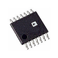
AD8343ARU-REEL Analog Devices Inc, AD8343ARU-REEL Datasheet - Page 16

AD8343ARU-REEL
Manufacturer Part Number
AD8343ARU-REEL
Description
IC MIXER ACTIVE HI-IP3 14-TSSOP
Manufacturer
Analog Devices Inc
Series
AD8343r
Datasheet
1.AD8343ARUZ.pdf
(32 pages)
Specifications of AD8343ARU-REEL
Rohs Status
RoHS non-compliant
Rf Type
Cellular, WLAN
Frequency
0Hz ~ 2.5GHz
Number Of Mixers
1
Gain
7dB
Noise Figure
14dB
Secondary Attributes
Up/Down Converter
Current - Supply
60mA
Voltage - Supply
4.5 V ~ 5.5 V
Package / Case
14-TSSOP (0.173", 4.40mm Width)
Operating Temperature (min)
-40C
Operating Temperature (max)
85C
Operating Temperature Classification
Industrial
Lead Free Status / Rohs Status
Not Compliant
Available stocks
Company
Part Number
Manufacturer
Quantity
Price
AD8343
DC INTERFACES
BIASING AND DECOUPLING (VPOS, DCPL)
VPOS is the power supply connection for the internal bias circuit
and the LO driver. Bypass this pin closely to GND with a
capacitor in the range of 0.01 μF to 0.1 μF. The DCPL pin
provides access to an internal bias node for noise bypassing
purposes. Bypass this node to COMM with 0.1 μF.
POWER-DOWN INTERFACE (PWDN)
The AD8343 is active when the PWDN pin is held low; other-
wise the device enters a low-power state as shown in Figure 51.
To assure full power-down, the PWDN voltage must be within
0.5 V of the supply voltage at VPOS. Normal operation requires
that the PWDN pin be taken at least 1.5 V below the supply
voltage. The PWDN pin sources about 160 μA when pulled to
GND (see the Pin Configuration and Function Descriptions
section). It is not advised to leave the pin floating when the
device is disabled; a resistive pull-up to VPOS is the minimum
suggestion.
The AD8343 requires about 2.2 μs to turn off when PWDN is
asserted; turn-on time is about 500 ns. Figure 52 and Figure 53
show typical characteristics (they vary with bypass component
values). Figure 54 shows the test configuration used to acquire
these waveforms.
45
40
35
30
25
20
15
10
5
0
3.0
Figure 51. Device Current vs. PWDN Voltage
3.5
POWER-DOWN VOLTAGE (V)
4.0
POWER-DOWN
SWEPT FROM
BOTH 3V TO 5V
AND 5V TO 3V
4.5
5.0
Rev. B | Page 16 of 32
VPOS
TRANSFORMER
NETWORK AND
1
2
1
2
GENERATOR
GENERATOR
MATCHING
HP8648C
CH1
SIGNAL
CH1
HP8130
PULSE
1nH
Figure 52. PWDN Response Time Device On to Off
Figure 53. PWDN Response Time Device Off to On
Figure 54. PWDN Response Time Test Schematic
RF INPUT
1740MHz
200nVΩ CH2 1.00VΩ
200nVΩ CH2 1.00VΩ
TRIGGER
0.1µF
0.1µF
1
2
3
4
5
6
7
OSCILLOSCOPE
COMM
INPP
INPM
DCPL
VPOS
PWDN
COMM
TEKTRONIX
AD8343
TDS694C
M500ns
M100ns
COMM
COMM
COMM
OUTM
OUTP
LOIM
LOIP
14
13
12
11
10
9
8
IF OUTPUT
CH2
CH2
170MHz
TRANSFORMER
TRANSFORMER
NETWORK AND
GENERATOR
MATCHING
HP8648C
SIGNAL
4.48V
4.48V
LO INPUT
1570MHz


