ATAKSTK511-8 Atmel, ATAKSTK511-8 Datasheet - Page 32
ATAKSTK511-8
Manufacturer Part Number
ATAKSTK511-8
Description
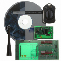
KIT RF MODULE 868MHZ FOR STK500
Manufacturer
Atmel
Series
SmartRF®r
Type
Transmitter, Receiver, ASK, FSKr
Specifications of ATAKSTK511-8
Frequency
868MHz
Wireless Frequency
868 MHz
For Use With/related Products
ATSTK500
Lead Free Status / RoHS Status
Contains lead / RoHS non-compliant


1925C–AVR–3/03
Hardware Description
3.8.5
3.8.6
3-22
BSEL2 Jumper
PJUMP Jumpers
Figure 3-30. XTAL1 and OSCSEL Connections
The BSEL2 jumper connects the Byte Select 2 signal for High-voltage Programming of
ATmega8, ATmega16, ATmega161, ATmega163, ATmega128, and ATmega323. The
BSEL2 jumper should only be mounted when High-voltage Programming ATmega16,
ATmega161, ATmega163, ATmega128, or ATmega323. When using ATmega8, con-
nect the right BSEL2 pin to PC2 in the target area. See Figure 3-31. For descriptions of
the Byte Select 2 signal, see the programming section of the corresponding parts
datasheet.
Figure 3-31. BSEL2 Connection for ATmega8
The PJUMP jumpers route the programming pin of AT90S2333, AT90S4433, and
ATmega8 to the programming lines when using High-voltage Programming. The
PJUMP jumpers should only be mounted when using High-voltage Programming on
AT90S2333, AT90S4433, or ATmega8. During debugging, High-voltage Programming
of other parts and ISP programming, these jumpers should not be mounted.
Figure 3-32. PJUMP Jumpers Placement
Cable to PC2
Studio
AVR
PJUMP
Oscillator
BSEL2
MASTER
MCU
OSCSEL
Jumper
3
2
1
Correct
Jumper
Placement
5V
Not
Correct
converter
Voltage
VTG
Jumper
XTAL1
AVR STK500 User Guide
GND
REF
PE0
PE2
XT1
PORTE
XTAL1 NET
1 2
PE1
RST
GND
XT2
VTG
Related parts for ATAKSTK511-8
Image
Part Number
Description
Manufacturer
Datasheet
Request
R

Part Number:
Description:
DEV KIT FOR AVR/AVR32
Manufacturer:
Atmel
Datasheet:

Part Number:
Description:
INTERVAL AND WIPE/WASH WIPER CONTROL IC WITH DELAY
Manufacturer:
ATMEL Corporation
Datasheet:
Part Number:
Description:
Low-Voltage Voice-Switched IC for Hands-Free Operation
Manufacturer:
ATMEL Corporation
Datasheet:
Part Number:
Description:
MONOLITHIC INTEGRATED FEATUREPHONE CIRCUIT
Manufacturer:
ATMEL Corporation
Datasheet:
Part Number:
Description:
AM-FM Receiver IC U4255BM-M
Manufacturer:
ATMEL Corporation
Datasheet:
Part Number:
Description:
Monolithic Integrated Feature Phone Circuit
Manufacturer:
ATMEL Corporation
Datasheet:
Part Number:
Description:
Multistandard Video-IF and Quasi Parallel Sound Processing
Manufacturer:
ATMEL Corporation
Datasheet:
Part Number:
Description:
High-performance EE PLD
Manufacturer:
ATMEL Corporation
Datasheet:
Part Number:
Description:
8-bit Flash Microcontroller
Manufacturer:
ATMEL Corporation
Datasheet:
Part Number:
Description:
2-Wire Serial EEPROM
Manufacturer:
ATMEL Corporation
Datasheet: