1321XEVK Freescale Semiconductor, 1321XEVK Datasheet - Page 51
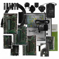
1321XEVK
Manufacturer Part Number
1321XEVK
Description
KIT EVALUATION FOR 1321X
Manufacturer
Freescale Semiconductor
Type
Zigbeer
Specifications of 1321XEVK
Frequency
2.4GHz
Wireless Frequency
2.4 GHz
Modulation
DSSS OQPSK
Security
128 bit AES
Operating Voltage
2 VDC to 3.4 VDC
Operating Temperature Range
- 40 C to + 85 C
For Use With/related Products
MC1321x
Lead Free Status / RoHS Status
Contains lead / RoHS non-compliant


1
2
3
4
5
6
Freescale Semiconductor
Input low voltage (V
Input low voltage (1.8 V ≤ V
Input hysteresis (all digital inputs)
Input leakage current (per pin)
High impedance (off-state) leakage current (per pin)
Internal pullup and pulldown resistors
Internal pulldown resistors (Port A4–A7 and IRQ)
Output high voltage (V
Output high voltage (ports C and F)
Maximum total I
Output low voltage (V
Output low voltage (ports C and F)
Maximum total I
dc injection current
Input capacitance (all non-supply pins)
Typicals are measured at 25°C.
This parameter is characterized and not tested on each device.
Measurement condition for pull resistors: V
Power supply must maintain regulation within operating V
conditions. If positive injection current (V
in external power supply going out of regulation. Ensure external V
current. This will be the greatest risk when the MCU is not consuming power. Examples are: if no system clock is present, or if
clock rate is very low which would reduce overall power consumption.
All functional non-supply pins are internally clamped to V
Input must be current limited to the value specified. To determine the value of the required current-limiting resistor, calculate
resistance values for positive and negative clamp voltages, then use the larger of the two values.
(all digital inputs)
(all port pins and IRQ)
I
I
I
I
I
I
Single pin limit
Total MCU limit, includes sum of all stressed pins
I
OH
OH
OH
OL
OL
OL
V
V
I
OL
OH
In
In
V
= 2.0 mA (ports A, B, D, E, and G)
= 6 mA (V
= 3 mA (V
= –10 mA (V
= –6 mA (V
= –3 mA (V
= 10.0 mA (V
= V
= V
= –2 mA (ports A, B, D, E, and G)
IN
< V
DD
DD
or V
or V
SS
OH
OL
DD
DD
, V
SS
SS,
DD
DD
for all port pins
IN
DD
for all port pins
≥ 2.3 V)
≥ 1.8 V)
DD
, all input/output
4, 5, 6, 7, 8
DD
all input only pins
≥ 2.3 V)
≥ 1.8 V)
> V
DD
≥ 2.7 V)
DD
≥ 2.7 V)
> 2.3 V) (all digital inputs)
≥ 1.8 V)
DD
≥ 1.8 V)
DD
Parameter
≤ 2.3 V)
Table 12. MCU DC Characteristics (continued)
(Temperature Range = –40 to 85°C Ambient)
3
(2)
MC13211/212/213 Technical Data, Rev. 1.8
In
> V
In
= V
DD
) is greater than I
SS
for pullup and V
SS
DD
and V
range during instantaneous and operating maximum current
DD
DD
DD
In
, the injection current may flow out of V
Symbol
.
|I
= V
V
load will shunt current greater than maximum injection
|I
R
R
V
V
I
|I
|I
OHT
C
V
V
OLT
OZ
hys
OH
IC
In
PU
PD
OL
IL
IL
In
DD
|
|
|
|
for pulldown.
0.06 × V
V
V
DD
DD
17.5
17.5
Min
—
—
—
—
—
—
—
—
—
—
—
—
—
– 0.5
– 0.5
DD
Typical
0.025
0.025
1
0.35 × V
0.30 × V
DD
Max
52.5
52.5
1.0
1.0
0.5
0.5
0.5
0.5
0.2
—
—
—
—
—
60
60
5
7
and could result
DD
DD
kohm
kohm
Unit
mA
mA
mA
mA
μA
μA
pF
V
V
V
V
V
51
Related parts for 1321XEVK
Image
Part Number
Description
Manufacturer
Datasheet
Request
R

Part Number:
Description:
Manufacturer:
Freescale Semiconductor, Inc
Datasheet:
Part Number:
Description:
Manufacturer:
Freescale Semiconductor, Inc
Datasheet:
Part Number:
Description:
Manufacturer:
Freescale Semiconductor, Inc
Datasheet:
Part Number:
Description:
Manufacturer:
Freescale Semiconductor, Inc
Datasheet:
Part Number:
Description:
Manufacturer:
Freescale Semiconductor, Inc
Datasheet:
Part Number:
Description:
Manufacturer:
Freescale Semiconductor, Inc
Datasheet:
Part Number:
Description:
Manufacturer:
Freescale Semiconductor, Inc
Datasheet:
Part Number:
Description:
Manufacturer:
Freescale Semiconductor, Inc
Datasheet:
Part Number:
Description:
Manufacturer:
Freescale Semiconductor, Inc
Datasheet:
Part Number:
Description:
Manufacturer:
Freescale Semiconductor, Inc
Datasheet:
Part Number:
Description:
Manufacturer:
Freescale Semiconductor, Inc
Datasheet:
Part Number:
Description:
Manufacturer:
Freescale Semiconductor, Inc
Datasheet:
Part Number:
Description:
Manufacturer:
Freescale Semiconductor, Inc
Datasheet:
Part Number:
Description:
Manufacturer:
Freescale Semiconductor, Inc
Datasheet:
Part Number:
Description:
Manufacturer:
Freescale Semiconductor, Inc
Datasheet: