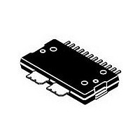
MWE6IC9100NR1 Freescale Semiconductor, MWE6IC9100NR1 Datasheet - Page 22

MWE6IC9100NR1
Manufacturer Part Number
MWE6IC9100NR1
Description
IC PWR AMP RF LDMOS TO270-14
Manufacturer
Freescale Semiconductor
Type
Power Amplifierr
Datasheet
1.MWE6IC9100GNR1.pdf
(23 pages)
Specifications of MWE6IC9100NR1
Frequency
960MHz
Gain
33.5dB
Package / Case
TO-270-14
Rf Type
GSM, EDGE
Voltage - Supply
28V
Number Of Channels
1
Frequency (max)
960MHz
Power Supply Requirement
Single
Single Supply Voltage (min)
26V
Single Supply Voltage (typ)
28V
Single Supply Voltage (max)
32V
Dual Supply Voltage (min)
Not RequiredV
Dual Supply Voltage (typ)
Not RequiredV
Dual Supply Voltage (max)
Not RequiredV
Mounting
Surface Mount
Lead Free Status / RoHS Status
Lead free / RoHS Compliant
Current - Supply
-
Noise Figure
-
P1db
-
Test Frequency
-
Lead Free Status / Rohs Status
Compliant
Available stocks
Company
Part Number
Manufacturer
Quantity
Price
Part Number:
MWE6IC9100NR1
Manufacturer:
FREESCALE
Quantity:
20 000
Application Notes
• AN1907: Solder Reflow Attach Method for High Power RF Devices in Plastic Packages
• AN1955: Thermal Measurement Methodology of RF Power Amplifiers
• AN1987: Quiescent Current Control for the RF Integrated Circuit Device Family
• AN3263: Bolt Down Mounting Method for High Power RF Transistors and RFICs in Over - Molded Plastic Packages
Engineering Bulletins
• EB212: Using Data Sheet Impedances for RF LDMOS Devices
MWE6IC9100NR1 MWE6IC9100GNR1 MWE6IC9100NBR1
22
Revision
Refer to the following documents to aid your design process.
The following table summarizes revisions to this document.
0
1
2
3
June 2007
Feb. 2007
Dec. 2008
May 2007
Date
• Initial Release of Data Sheet
• Changed Device box to 960 MHz to reflect functional test frequency, p. 1
• Added Power Added Efficiency to GSM EDGE Application Typical Performances, p. 1
• Changed “5:1 VSWR, @ 28 Vdc” to “10:1 VSWR, @ 32 Vdc” in the Capable of Handling bullet, p. 1
• Added Footnote (1) to Quiescent Current Thermal Tracking bullet under Features section and to
• Added top - level, 2 - stage block diagram depiction to Fig. 2, Pin Connections; updated Note, p. 1
• Added Case Operating Temperature limit to the Maximum Ratings table and set limit to 150°C, p. 2
• Added Stage 1 and Stage 2 DC Electrical Characteristics tables, p. 2, 3
• In Table 6, Component Designations and Values, corrected Part Number ATC100B331JT500XT to
• Updated Figs. 7 and 8, Power Gain versus Output Power, to remove non - variable I
• Updated Fig. 9, Intermodulation Distortion Products versus Output Power, to show PEP and not CW;
• Updated graphical representation of Ideal/Actual in Fig. 11, Pulsed CW Output Power versus Input Power,
• Removed Case Operating Temperature from Maximum Ratings table, p. 2. Case Operating Temperature
• Changed full frequency band in Typical GSM Performance bullet to f = 960 MHz to match actual production
• Changed Storage Temperature Range in Max Ratings table from - 65 to +200 to - 65 to +150 for
• Added Case Operating Temperature limit to the Maximum Ratings table and set limit to 150°C, p. 2
• Operating Junction Temperature increased from 200°C to 225°C in Maximum Ratings table, related
• Corrected Z10 from 1.17” to 0.117” in the Test Circuit Schematic Z list, p. 4
• Updated Part Numbers in Table 6, Component Designations and Values, to latest RoHS compliant part
• Replaced Case Outline 1617 - 01 with 1617 - 02, Issue A, p. 1, 13 - 15. Revised cross - hatched area for
• Replaced Case Outline 1618 - 01 with 1618 - 02, Issue A, p. 1, 16 - 18. Added pin numbers 1, 12, 13, and 14
• Replaced Case Outline 1621 - 01 with 1621 - 02, Issue A, p. 1, 19 - 21. Added pin numbers 1, 12, 13, and 14
• Added Product Documentation and Revision History, p. 22
Quiescent Current Temperature Compensation in Fig. 1, Functional Block Diagram, p. 1
ATC100B331JT200XT for C24 capacitor, p. 4
corrected frequency value to show 100 kHz Tone Spacing, p. 7
to show correct 3 and 6 dB compression points, p. 7
rating will be added to the Maximum Ratings table when parts’ Operating Junction Temperature is
increased to 225°C.
test, p. 1
standardization across products, p. 2
“Continuous use at maximum temperature will affect MTTF” footnote added and changed 200°C to 225°C
in Capable Plastic Package bullet, p. 1, 2
numbers, p. 4
exposed heat spreader. Added pin numbers 1, 12, 13, and 14 to Sheets 1 and 2. Corrected mm Min and
Max values for dimension A1 to 0.99 and 1.09, respectively.
and Pin 1 Index designation to Sheet 1. Corrected dimensions e and e1 on Sheet 1. Removed Pin 5
designation from Sheet 2.
and Pin 1 Index designation to Sheet 1. Corrected dimensions e and e1 on Sheets 1 and 3. Removed Pin 5
designation from Sheet 2.
PRODUCT DOCUMENTATION
REVISION HISTORY
Description
Freescale Semiconductor
DQ
value, p. 6
RF Device Data


